TD62082A View Datasheet(PDF) - Toshiba
Part Name
Description
Manufacturer
TD62082A Datasheet PDF : 11 Pages
| |||
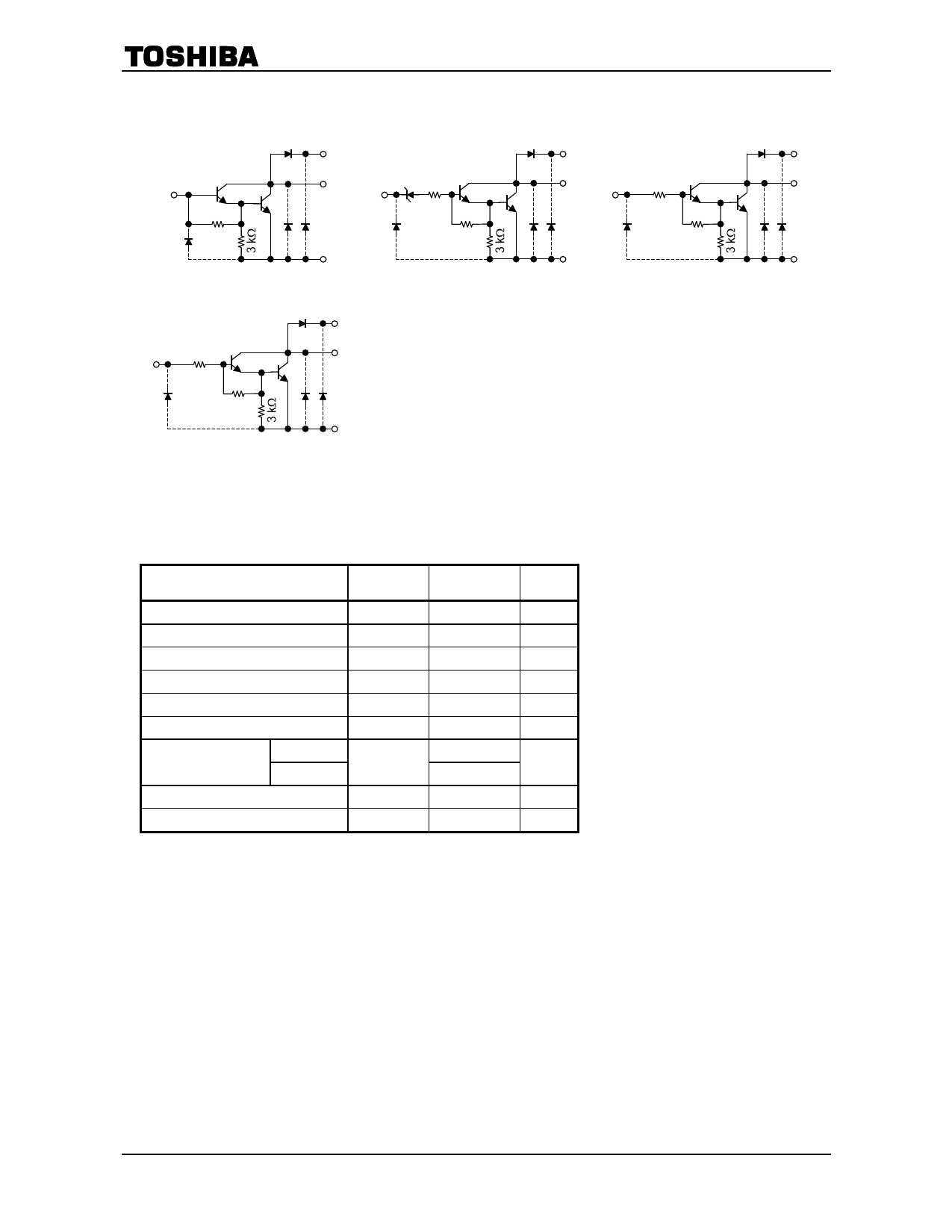
Schematics (each driver)
TD62081~084AP/AF
TD62081AP/AF Common
TD62082AP/AF Common
TD62083AP/AF Common
Input
7.2 kΩ
Output
Input 7 V
10.5 kΩ
7.2 kΩ
GND
TD62084AP/AF Common
Input
Output
2.7 kΩ
7.2 kΩ
GND
Output
GND
Input
10.5 kΩ
7.2 kΩ
Output
GND
Note: The input and output parasitic diodes cannot be used as clamp diodes.
Maximum Ratings (Ta = 25°C)
Characteristics
Output sustaining voltage
Output current
Input voltage
Input current
Clamp diode reverse voltage
Clamp diode forward current
AP
Power dissipation
AF
Operating temperature
Storage temperature
Note 1: Except TD62081AP/AF
Note 2: Only TD62081AP/AF
Symbol
VCE (SUS)
IOUT
VIN (Note 1)
IIN (Note 2)
VR
IF
PD
Topr
Tstg
Rating
−0.5 to 50
500
−0.5 to 30
25
50
500
1.47
0.96
−40 to 85
−55 to 150
Unit
V
mA/ch
V
mA
V
mA
W
°C
°C
2
2005-04-15
Share Link: 