EM25LV512-25MS View Datasheet(PDF) - ELAN Microelectronics
Part Name
Description
Manufacturer
EM25LV512-25MS Datasheet PDF : 30 Pages
| |||
EM25LV512
512 K (64K x 8) Bits Serial Flash Memory
SPECIFICATION
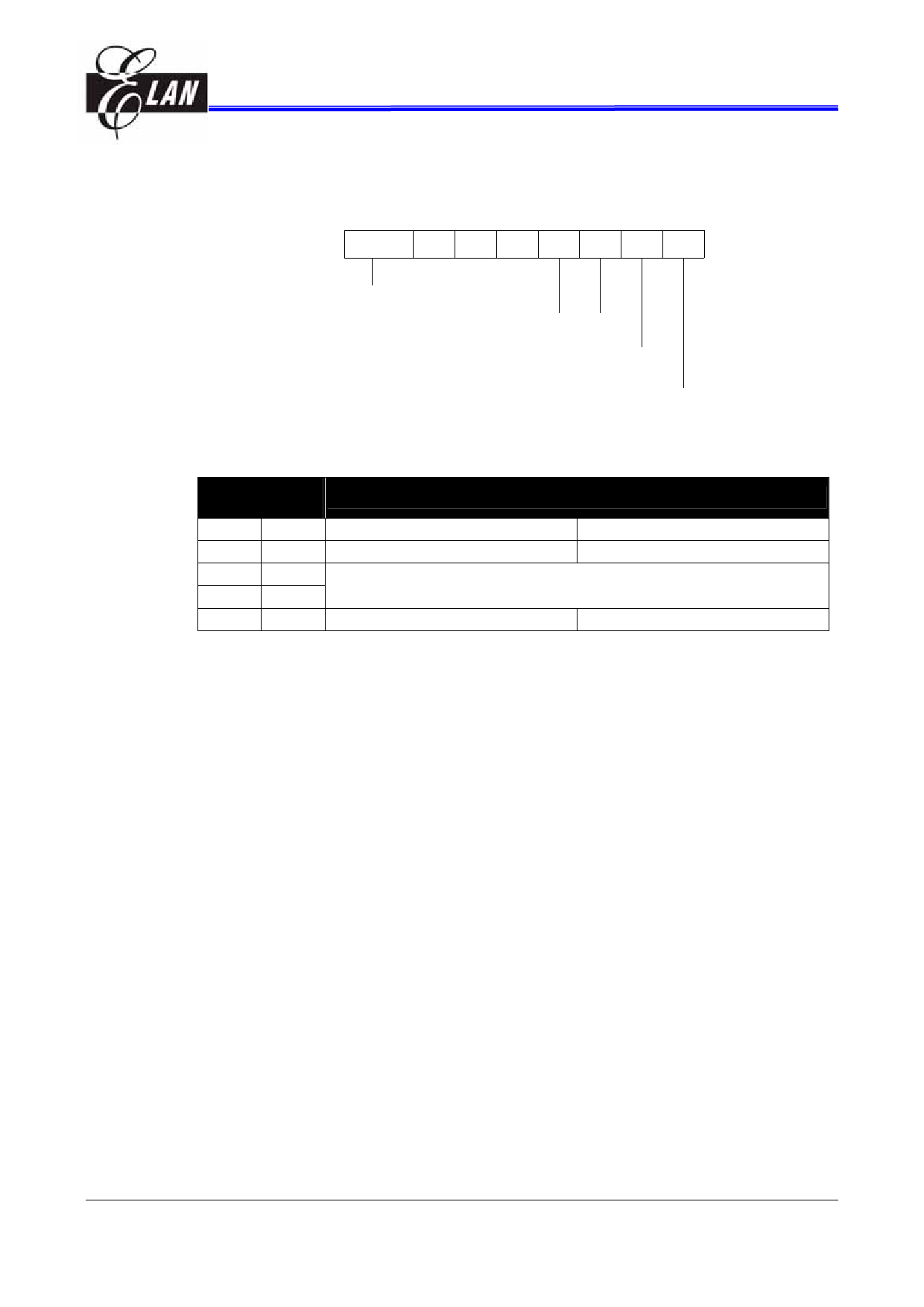
b7
b0
SRWD 0 0 0 BP1 BP0 WEL BUSY
Status Register Write Protect
Block Protect Bits
Write Enable Latch Bit
BUSY Bit
Table 3: Status Register Format
Status Register
Content
Memory Contents
BP1 Bit BP0 Bit Protected Area
0
0 None
Unprotected Area
All blocks* (2 blocks: 0 & 1)
0
1 No protection against Page Program (PP) and Block Erase (BE)
1
0
All blocks (Block 0 and 1) protected against Chip Erase (CE)
1
1 All blocks (2 blocks: 0 & 1)
None
* The device is ready to accept a Chip Erase instruction provided that both Block Protects
(BP1 and BP0) are set to “0”.
Table 4: Protected Area Sizes
This specification is subject to change without further notice. (11.08.2004 V1.0)
Page 7 of 30
Share Link: 