MB40166 View Datasheet(PDF) - Fujitsu
Part Name
Description
Manufacturer
MB40166 Datasheet PDF : 20 Pages
| |||
MB40166/MB40176
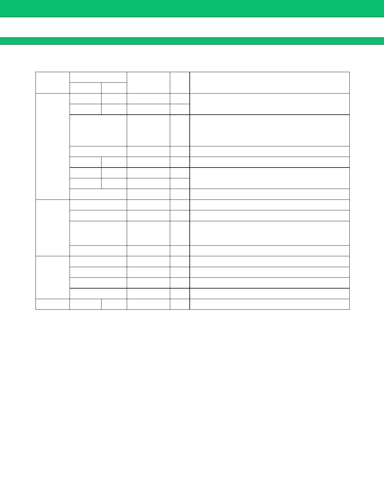
s PIN DESCRIPTIONS
Section
Pin No.
40166 40176
21
–
–
19
Symbol
VINA
VIN
A/D
D/A
Common
Other
22
8 to 13
20
–
–
20
–
21
14
24
2 to 7
23
1
18, 25
16, 27
17, 26
15, 28
19
–
VREF
DA1 to DA6
VCLMP
C1
C2
ADCK
VOUT
DD1 to DD6
COMP
DACK
VCCA
VCCD
A.GND
D.GND
(N.C.)
I/O
Function
I
Analog signal input.
I
Reference voltage output.
O
Reference voltage divided by the resistors, with the
output
voltage set to 0.8 x VCCA (V).
O Digital signal outputs. (DA1: MSB, DA6: LSB)
O Clamp voltage output.
–
Clamp capacitor is connected between these pins.
–
I A/D conversion clock input.
O Analog signal output.
I Digital signal input. (DD1: MSB, DD6: LSB)
Phase compensation capacitor is connected.
– Insert a capacitor of 1 µF or more between this pin and
A.GND.
I D/A conversion clock input.
– Power supply for analog circuit. (+5 V)
– Power supply for digital circuit. (+5 V)
– Ground for analog circuit. (0 V)
– Ground for digital circuit. (0 V)
– No connection.
5
Share Link: 