MC33565DR2 View Datasheet(PDF) - ON Semiconductor
Part Name
Description
Manufacturer
MC33565DR2 Datasheet PDF : 12 Pages
| |||
MC33565
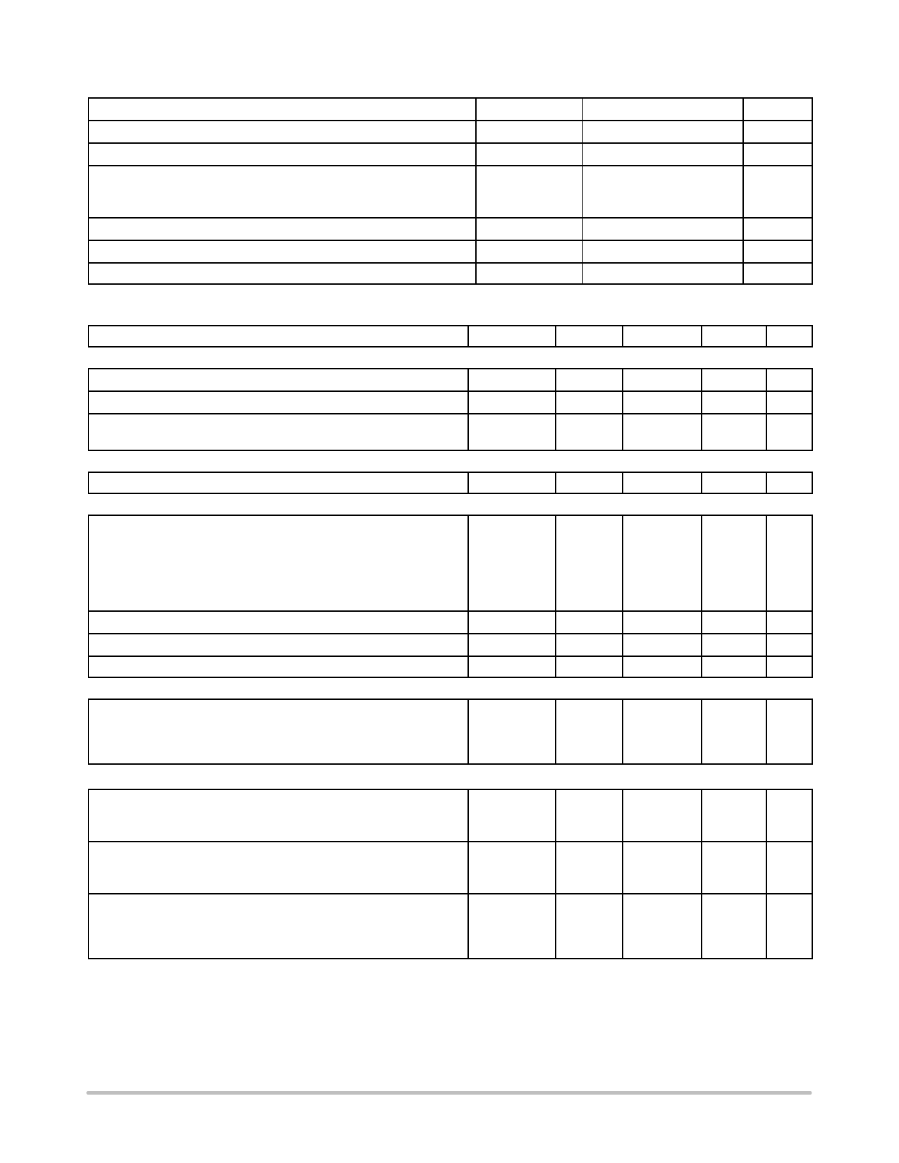
MAXIMUM RATINGS (Notes 1, 2)
Rating
Symbol
Value
Unit
Main Input Voltage Range (Pin 1)
Auxiliary Input Voltage Range (Pin 3)
Thermal Resistance Junction to Air
D Suffix, SOIC–8, Case 751
DM Suffix, MSOP–8, Case 846A
Vin(M)
Vin(A)
RθJA
–0.5 to +7.0
–0.5 to +7.0
146
172
V
V
°C/W
Operating Junction Temperature Range
Storage Temperature Range
Lead Temperature (Soldering, 10 seconds)
TJ
–5.0 to +150
°C
Tstg
–55 to +150
°C
TL
300
°C
ELECTRICAL CHARACTERISTICS (Vin(A) = 3.3 V, Vin(M) = 5.0 V, Pin 6 connected to Pin 7, Cpin6,7 = 4.7 mF, for typical values
TJ = 25°C, for min/max values TJ = –5.0°C to 150°C unless otherwise noted.)
Characteristic
Symbol
Min
Typ
Max
Unit
MAIN INPUT (Pin 1)
Operating Voltage Range
Quiescent Current (IO = 0 mA)
Output to Input Reverse Leakage Current
(Vin(M) = 0 V, Vout = 3.5 V, TJ = 25°C)
AUXILIARY INPUT (Pin 3)
Quiescent Current (IO = 0 mA)
REGULATOR OUTPUT (Pin 7)
Output Voltage (IO = 0 mA to 200 mA, Note 3)
Vin(M) = 4.3 V to 5.5 V
TA = 25°C
TJ = –5.0°C to 150°C
Vin(M) = Vth(L)
Vin(M) = 7.0 V
Line Regulation
Load Regulation
Short Circuit Current (TJ = 25°C, Note 3)
LOW VOLTAGE DETECTOR (Pins 1, 8)
Input Threshold Voltage (Figure 3)
Output Low State Transition, Vin(M) Decreasing
Output High State Transition, Vin(M) Increasing
Hysteresis
Vin(M)
4.3
5.0
5.5
V
IQ(M)
–
8.0
10
mA
IL
–
1.4
25
µA
IQ(A)
Vout
Regline
Regload
ISC
Vth(L)
Vth(H)
VH
–
3.267
3.234
3.0
3.1
–
–
230
3.9
–
0.120
1.9
3.3
3.3
–
3.3
1.5
1.9
750
4.02
4.17
0.150
3.0
mA
V
3.333
3.366
–
3.5
13.2
mV
13.2
mV
800
mA
V
4.3
4.3
0.180
SWITCH DRIVE OUTPUT (Pin 8)
Output Voltage
Low State (Vin(M) = 0 V, Vin(A) = 3.3 V, Isink = 200 mA)
High State (Vin(M) = 5.0 V, Vin(A) = 0 V, Isource = 200 mA)
VO(L)
VO(H)
–
0.044
3.4
4.15
Peak Output Current (CL = 1.2 nF)
Sink Current (Vin(M) = 3.9 V, VO = 1.0 V)
Source Current (Vin(M) = 4.3 V, VO = 2.3 V)
Isink(PK)
15
22
Isource(PK)
15
39
Propagation Delay, Main Input to Switch Drive Output (Figure 4)
CL = 1.2 nF
Switch Drive Output Fall (Vin(M) Decreasing)
Switch Drive Output Rise (Vin(M) Increasing)
tDL
–
0.65
tDH
–
1.4
1. Maximum Ratings are those values beyond which damage to the device may occur.
2. This device series contains ESD protection and exceed the following tests:
Human Body Model 2500 V per MIL STD 883, Method 3015.
Machine Model Method 400 V.
3. Thermal shutdown activation can occur when the maximum operating junction temperature is exceeded.
V
0.2
–
mA
–
–
ms
3.5
3.5
http://onsemi.com
3
Share Link: 