OPB702 View Datasheet(PDF) - Optek Technology
Part Name
Description
Manufacturer
OPB702 Datasheet PDF : 4 Pages
| |||
Type OPB702
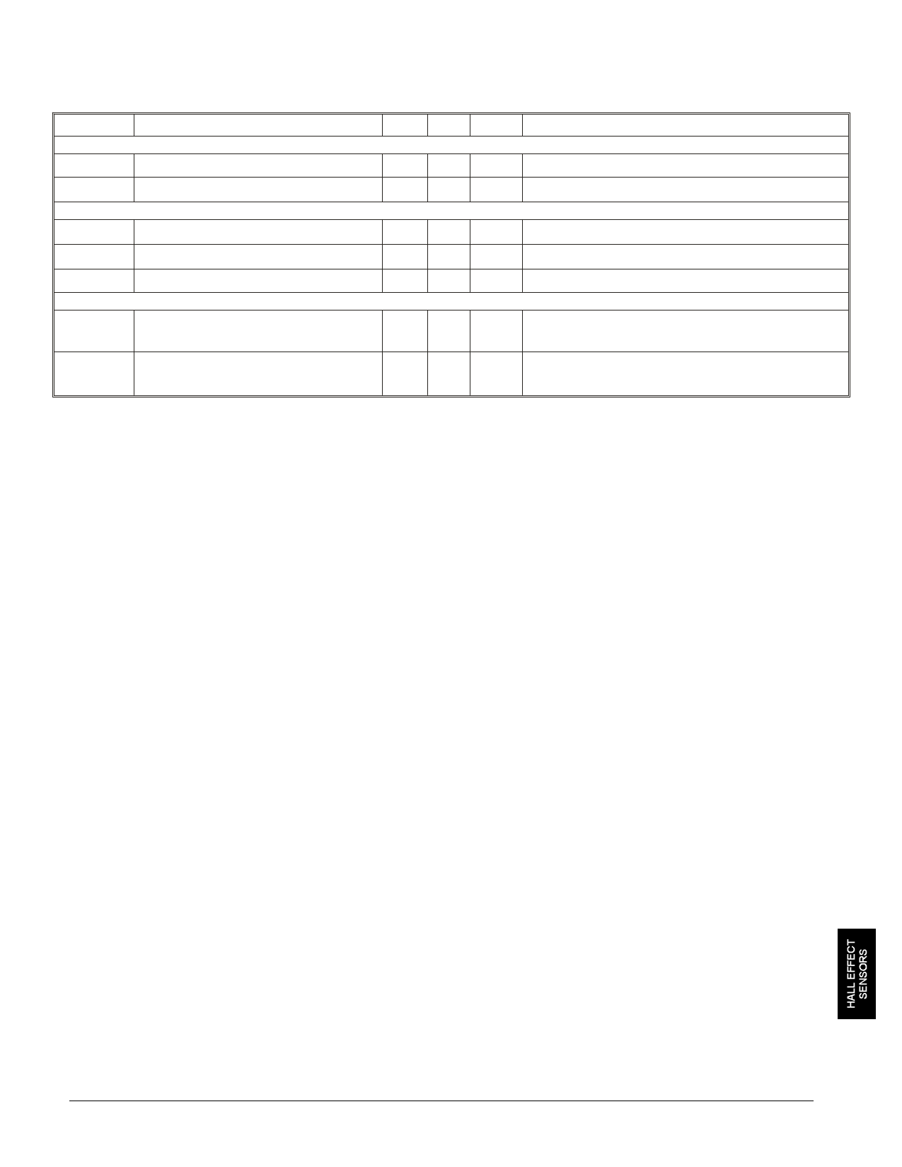
Electrical Characteristics (TA = 25°C unless otherwise noted)
SYMBOL
PARAMETER
Input Diode
VF
Forward Voltage
IR
Reverse Current
Output Phototransistor
V(BR)CEO Collector-Emitter Breakdown Voltage
V(BR)ECO Emitter-Collector Breakdown Voltage
ICEO
Coupled
Collector-Emitter Leakage Current
IC(ON) On-State Collector Current
Collector-Emitter Saturation Voltage
VCE(SAT)
MIN MAX UNITS
TEST CONDITIONS
1.8
V IF = 20 mA
100 µA VR = 2.0 V
30
5.0
100
V IC = 100 µA, IF = 0, Ee = 0
V IE = 100 µA, IF = 0, Ee = 0
nA VCE = 10 V, IF = 0, Ee = 0
50
0.40
µA
VCE = 5.0 V, IF = 40 mA,
d = 0.150”(3.81 mm)(3)(4)
V
IC = 250 µA, IF = 40 mA,
d = 0.150”(3.81 mm)(3)(4)
Optek reserves the right to make changes at any time in order to improve design and to supply the best product possible
Optek Technology, Inc. 1215 W. Crosby Road Carrollton, Texas 75006
(972)323-2200
Fax (972)323-2396
Share Link: 