MX23C8000TC-12 View Datasheet(PDF) - Macronix International
Part Name
Description
Manufacturer
MX23C8000TC-12 Datasheet PDF : 11 Pages
| |||
PIN DESCRIPTION
Symbol
A0~A19
Q0~Q7
CE
OE
VCC
VSS
Pin Function
Address Inputs
Data Outputs
Chip Enable Input
Output Enable Input
Power Supply Pin (+5V)
Ground Pin
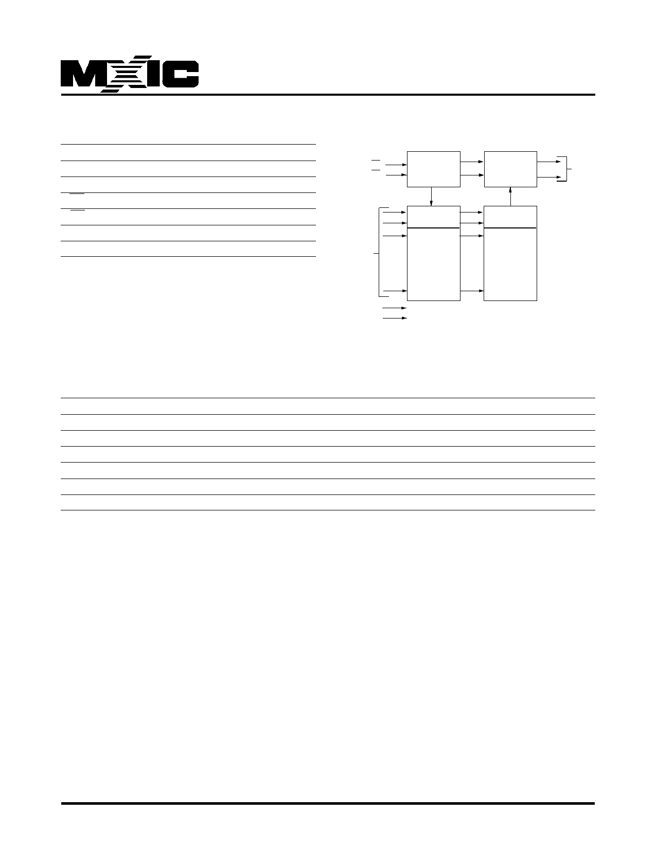
MX23C8000
BLOCK DIAGRAM
CE
CONTROL
OE
LOGIC
OUTPUT
BUFFERS
.
.
.
A0~A19
.
ADDRESS
.
INPUTS
.
.
.
VCC
VSS
Y-DECODER
.
.
.
.
.
X-DECODER
.
.
.
Y-SELECT
8M BIT
ROM ARRAY
Q0~Q7
ABSOLUTE MAXIMUM RATINGS
RATING
Ambient Operating Temperature
Storage Temperature
Applied Input Voltage
Applied Output Voltage
VCC to Ground Potential
Power Dissipation
VALUE
0° C to 70° C
-65° C to 125° C
-0.5V to VCC+0.5
-0.5V to VCC+0.5
-0.5V to 7.0V
1.0W
Note: minimum DC voltage on input or I/O pins is -0.5V. During voltage transitions, inputs may undershoot VSS to -
2.0V for periods of up to 20ns. Maximum DC voltage on input or I/O pins is VCC+0.5V. During voltage transitions,
input may overshoot VCC to VCC+2.0V for periods of up to 20ns.
P/N:PM0137
REV. 4.3, JUL. 03, 2003
2
Share Link: 