SY89424V View Datasheet(PDF) - Micrel
Part Name
Description
Manufacturer
SY89424V Datasheet PDF : 5 Pages
| |||
Micrel
ClockWorks™
SY89424V
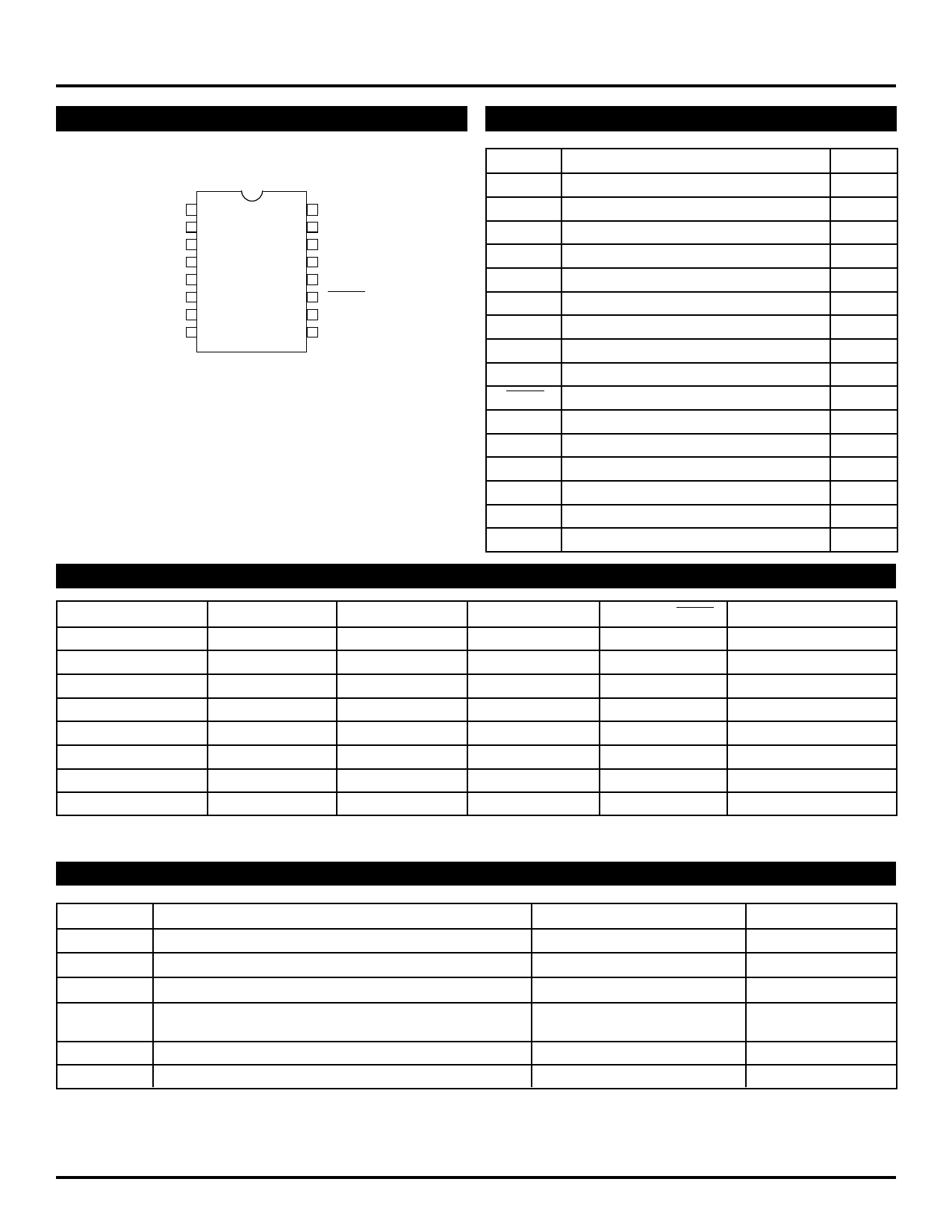
PIN CONFIGURATION
PIN NAMES
VCCQ
XTAL2
VEE
XTAL1
S1
VCC
S3
S2
1
16
2
15
3
14
4 Top View 13
5 Gullwing 12
6
11
7
10
8
9
F1
F2
OE
PDR1
FOUT
FOUT
PDR2
VCCO
FREQUENCY SELECTION TABLE
Input
S1
S2
FOSC(1)
0
0
0
0
0
1
0
1
1
0
1
0
1
1
1
1
NOTE:
1. FOSC = 10MHz to 25MHz.
ABSOLUTE MAXIMUM RATING(1)
Pin
Function
I/O
XTAL1 Crystal Input 1
(PECL)
I/O
XTAL2 Crystal Input 2
(PECL)
I/O
F1
Filter Pin 1
—
F2
Filter Pin 2 (Reference)
—
VCCQ
Positive Power Supply (Charge Pump)
—
S1
Select Input 1
(TTL)
I
S2
Select Input 2
(TTL)
I
S3
Select Input 3
(TTL)
I
FOUT
Output
(PECL)
O
FOUT
Complement Output (PECL)
O
VCC
Positive Power Supply (Logic)
—
VCCO
Positive Power Supply (PECL Outputs) —
OE
Output Enable
(TTL)
I
VEE
Negative Power Suppy (0.0V)
—
PDR1
Pulldown Resistor (100Ω)
—
PDR2
Pulldown Resistor (100Ω)
—
S3
FOUT, FOUT Frequency Range MHz
0
24X FOSC
240 – 480
1
12X FOSC
120 – 240
0
8X FOSC
80 – 160
1
6X FOSC
60 – 120
0
50X FOSC
500 – 1000
1
25X FOSC
250 – 500
0
16.67X FOSC
167 – 333
1
12.5X FOSC
125 – 250
Symbol
Parameter
Value
Unit
VCC
Power Supply Voltage
–0.5 to +7.0
V
VI
TTL Input Voltage(2)
–0.5 to 6.0
V
II
TTL Input Current(2)
–30 to +5.0
mA
IOUT
ECL Output Current
–Continuous
50
mA
–Surge
100
Tstore
Storage Temperature
–65 to +150
°C
TA
Operating Temperature
0 to +75
°C
NOTES:
1. Permanent device damage may occur if ABSOLUTE MAXIMUM RATINGS are exceeded. This is a stress rating only and functional operation is not
implied at conditions other than those detailed in the operational sections of this data sheet. Exposure to ABSOLUTE MAXIMUM RATING conditions
for extended periods may affect device reliability.
2. Either voltage limit or current limit is sufficient to protect input.
2
Share Link: 