UPD7759C View Datasheet(PDF) - NEC => Renesas Technology
Part Name
Description
Manufacturer
UPD7759C Datasheet PDF : 18 Pages
| |||
µPD7759
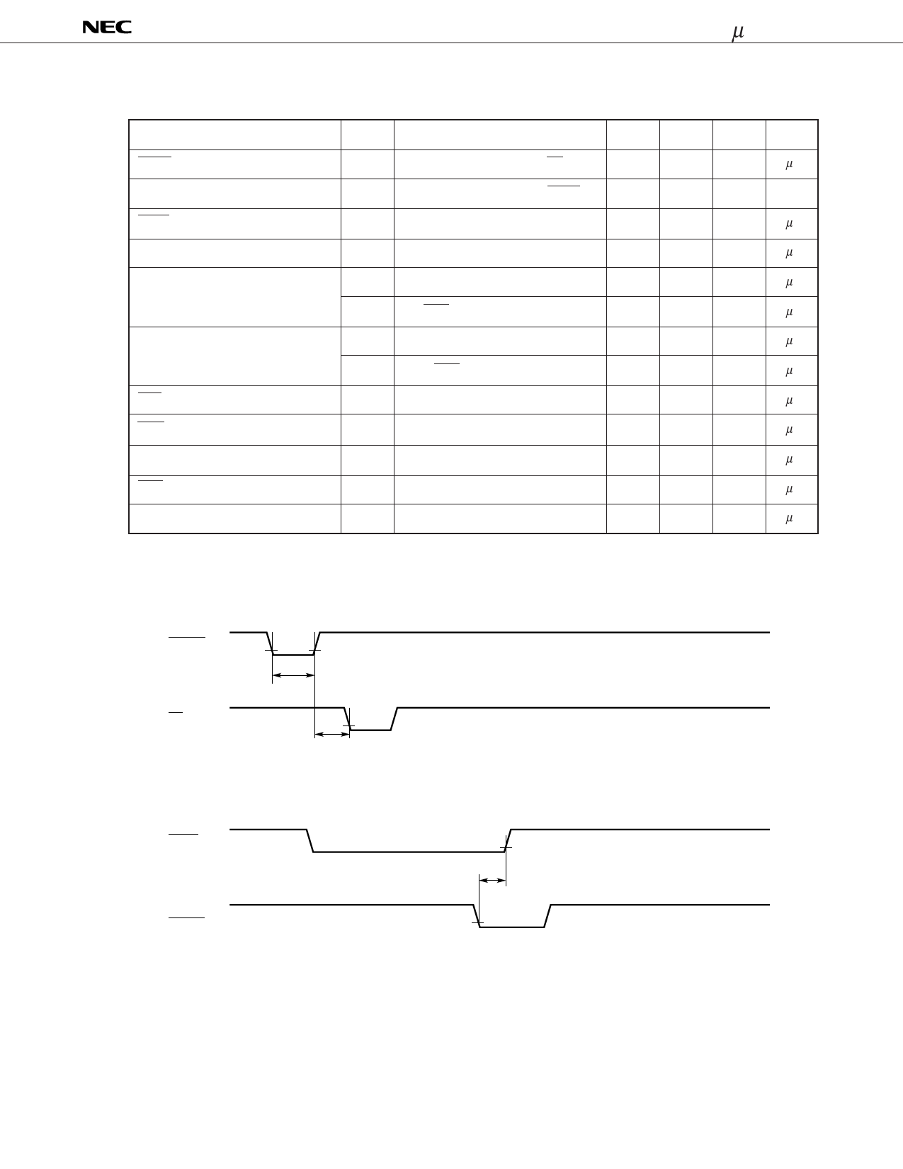
(2) SWITCHING CHARACTERISTICS
Parameters
BUSY output delay
Speech output delay
BUSY hold time
ALE pulse width
Higher address set up time
Higher address hold time
AEN pulse width
DRQ output delay
Higher address pulse width
DRQ pulse width
ROM read cycle time
Symbol
Conditions
tSBO In operation mode, from ST ↓
tSSO In operation mode, from BUSY ↓
tBD from synthesis
tLL
tAL
for ALE ↓
tAE
for AEN ↓
tLA
from ALE ↓
tEA
from AEN ↑
tAEN
tLC
from ALE ↓
tAC
tDCC
tMRO
MIN.
TYP.
6.25
2.1
3.13
3.13
0
3.13
0
14.1
3.13
6.25
7.81
37.5
MAX.
10
2.2
15
Unit
µs
ms
µs
µs
µs
µs
µs
µs
µs
µs
µs
µs
µs
TIMING CHART (at reset)
(1)
RESET
tRST
ST
tRS
(2)
BUSY
tRB
RESET
9
Share Link: 