UPSD3253B-40 View Datasheet(PDF) - STMicroelectronics
Part Name
Description
Manufacturer
UPSD3253B-40
STMicroelectronics

UPSD3253B-40 Datasheet PDF : 176 Pages
| |||
µPSD325X DEVICES
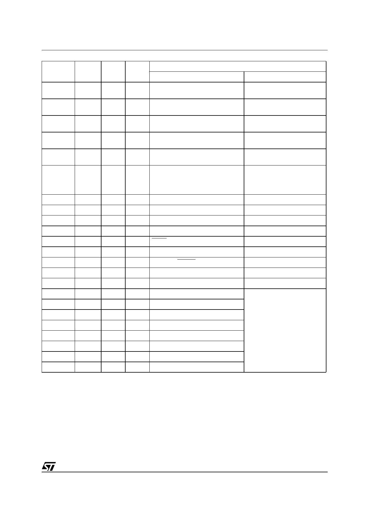
Port Pin
P4.3
P4.4
P4.5
P4.6
P4.7
PA0
PA1
PA2
PA3
PA4
PA5
PA6
PA7
Signal
Name
Pin No.
In/Out
Basic
Function
Alternate
PWM0
27
I/O General I/O port pin
8-bit Pulse Width Modulation
output 0
PWM1
25
I/O General I/O port pin
8-bit Pulse Width Modulation
output 1
PWM2
23
I/O General I/O port pin
8-bit Pulse Width Modulation
output 2
PWM3
19
I/O General I/O port pin
8-bit Pulse Width Modulation
output 3
PWM4
18
I/O General I/O port pin
Programmable 8-bit Pulse Width
modulation output 4
USB-
8
USB Pin Pull-up resistor required
I/O
(2kΩ for 3V devices, 7.5kΩ for 5V
devices) for all devices, with or
without USB function.
USB+
10
I/O USB Pin
AVREF 70
O Reference Voltage input for ADC
RD_
65
O READ signal, external bus
WR_
62
O WRITE signal, external bus
PSEN_ 63
O PSEN signal, external bus
ALE
4
O Address Latch signal, external bus
RESET_ 68
I Active low RESET input
XTAL1
48
I Oscillator input pin for system clock
XTAL2
49
O Oscillator output pin for system clock
35
I/O General I/O port pin
34
I/O General I/O port pin
32
I/O General I/O port pin
28
I/O General I/O port pin
26
I/O General I/O port pin
24
I/O General I/O port pin
1. PLD Macro-cell outputs
2. PLD inputs
3. Latched Address Out (A0-A7)
4. Peripheral I/O Mode
22
I/O General I/O port pin
21
I/O General I/O port pin
15/176
Share Link: