M50FW002 View Datasheet(PDF) - STMicroelectronics
Part Name
Description
Manufacturer
M50FW002 Datasheet PDF : 39 Pages
| |||
M50FW002
MAXIMUM RATING
Stressing the device above the rating listed in the
Absolute Maximum Ratings table may cause per-
manent damage to the device. Exposure to Abso-
lute Maximum Rating conditions for extended
periods may affect device reliability. These are
stress ratings only and operation of the device at
these or any other conditions above those indicat-
ed in the Operating sections of this specification is
not implied. Refer also to the STMicroelectronics
SURE Program and other relevant quality docu-
ments.
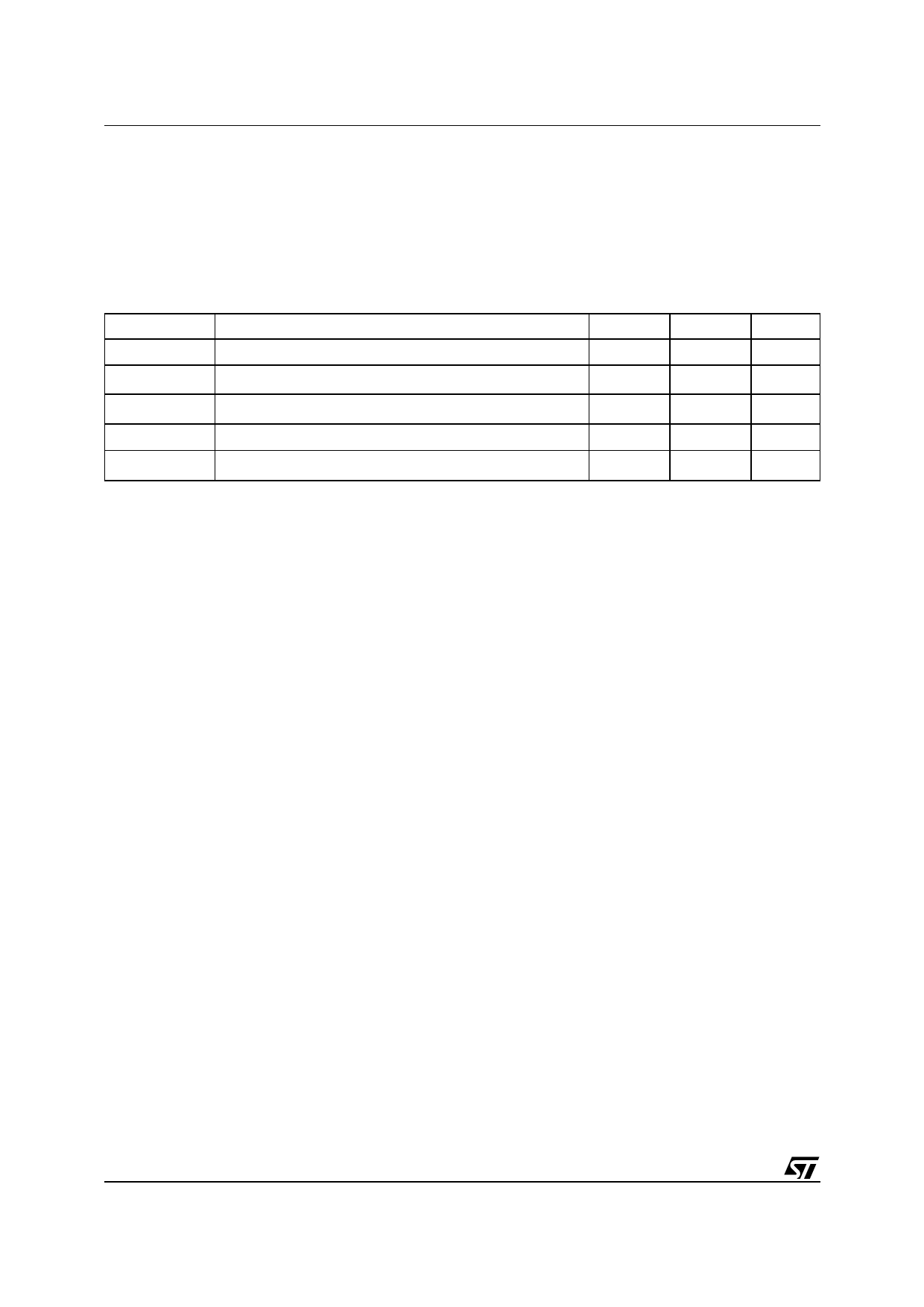
Table 14. Absolute Maximum Ratings
Symbol
Parameter
Min
Max
TBIAS
Temperature Under Bias
–50
125
TSTG
Storage Temperature
–65
150
VIO
Input or Output Voltage (1,2)
–0.6
VCC +0.6
VCC
Supply Voltage
–0.6
4
VPP
Program Voltage
–0.6
13
Note: 1. Minimum voltage may undershoot to –2V during transition and for less than 20ns during transitions.
2. Maximum voltage may overshoot to VCC +2V during transition and for less than 20ns during transitions.
Unit
°C
°C
V
V
V
20/39
Share Link: 