AN17820B View Datasheet(PDF) - Panasonic Corporation
Part Name
Description
Manufacturer
AN17820B
Panasonic Corporation

AN17820B Datasheet PDF : 16 Pages
| |||
AN17820B
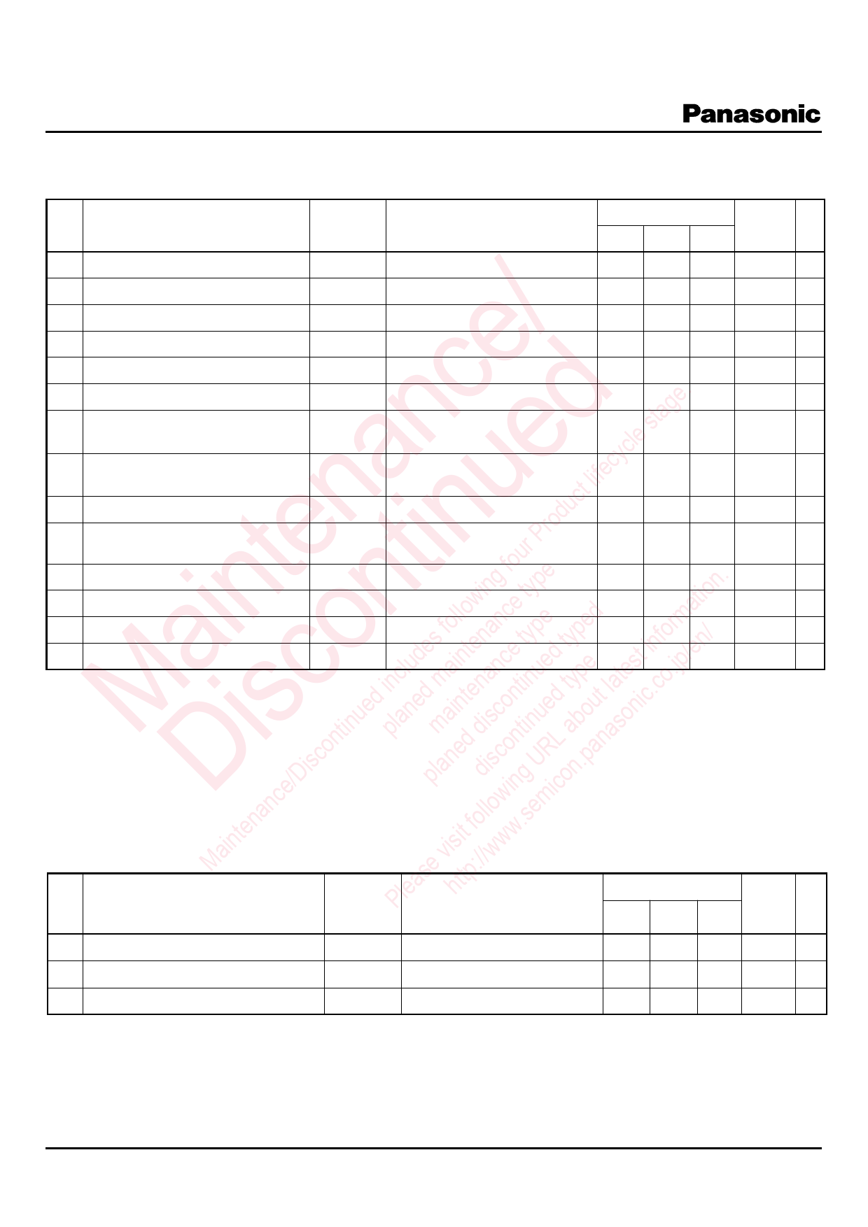
Electrical Characteristics at VCC = 12.0 V
Note) Unless otherwise specified, Ta = 25°C±2°C, Frequency = 1 kHz, RL = 8 Ω.
B
No.
Parameter
Symbol
Conditions
Limits
Min Typ Max
Unit
No
te
1 Quiescent circuit current
ICQ
Vin = 0 V, Vol = 0 V
— 45 100 mA —
2 Standby current
ISTB Vin = 0 V, Vol = 0 V
—
1
10
μA —
3 Output noise voltage
VNO Vol = 0 V, Rg = 10 kΩ
— 0.25 0.6 mV[rms] *
/ 4 Voltage gain
GV
PO = 1.0 W, Vol = 1.25 V
38 40 42
dB —
5 Total harmonic distortion
e . 6 Maximum power output 1
nc d stage 7 Maximum power output 2
a e lifecycle 8 Ripple rejection ratio
n u uct 9 Output offset voltage
THD
PO1
PO2
RR
VOFF
PO = 1.0 W, Vol = 1.25 V
THD = 10%, Vol = 1.25 V
VCC = 15 V,
THD = 10%, Vol = 1.25 V
Rg = 10 kΩ, Vol = 0 V,
Vr = 1 V[rms], fr = 120 Hz
Vol = 0 V, Rg = 10 kΩ
Prod 10 Volume attenuation ratio
Att PO = 1.0 W, Vol = 0 V
te ting four e . 11 Channel balance 1
CB1 PO = 1.0 W, Vol = 1.25 V
in n llowin e typ tion 12 Channel balance 2
CB2 PO = 1.0 W, Vol = 0.6 V
es fo tenanc type typed forma 13 Middle voltage gain
Gvm PO = 1.0 W, Vol = 0.6 V
a o lud in ce d t in /en/ 14 Channel crosstalk
CT PO = 1.0 W, Vol = 1.25 V
c ed inc ed ma tenan tinue type lates o.jp Note) *: For this measurement, use the BPF = 15 Hz to 30 kHz (12 dB/OCT).
— 0.15 0.5
6.0 7.5 —
10.0 12.5 —
30 50 —
–350 0 350
70 80 —
–1 0
1
–2 0
2
26.5 29.5 32.5
40 55 —
M Disance/Discontinu plan pmlaaniend ddlilisosccwooinnngtineUumReidLcoanb.opuatnasonic.c Electrical Characteristics (Reference values for design) at VCC = 12.0 V
ten fo .s Note) Unless otherwise specified, Ta = 25°C±2°C, Frequency = 1 kHz, RL = 8 Ω.
in isit ww The characteristics listed below are reference values for design of the IC and are not guaranteed by inspection.
Ma e v ://w If a problem does occur related to these characteristics, Panasonic will respond in good faith to user concerns.
leas http B
P No.
Parameter
Symbol
Conditions
Limits
Min Typ Max
%
W
W
dB
mV
dB
dB
dB
dB
dB
Unit
—
—
—
*
—
*
—
—
—
—
No
te
15 Standby pin current
16 Volume pin current
17 Input impedance
ISTB2
IVOL
Zi
Vin = 0 V, VSTB = 3.0 V
Vin = 0 V, Vol = 0 V
Vin = ±0.3 VDC
— — 25 μA —
–12 — — μA —
24 30 36 kΩ —
SDB00167BEB
7
Share Link: