HEF4521B View Datasheet(PDF) - NXP Semiconductors.
Part Name
Description
Manufacturer
HEF4521B Datasheet PDF : 18 Pages
| |||
NXP Semiconductors
HEF4521B
24-stage frequency divider and oscillator
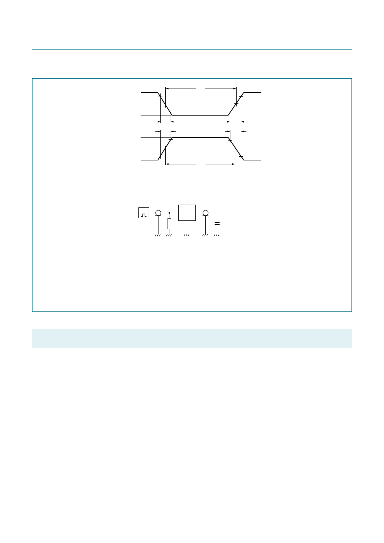
a. Input waveforms
VI
negative
pulse
0V
VI
positive
pulse
0V
90 %
10 %
VM
10 %
tf
tr
90 %
VM
tW
90 %
VM
10 %
tr
tf
90 %
VM
10 %
tW
001aaj781
VDD
VI
G
VO
DUT
RT
CL
001aag182
b. Test circuit
Fig 6.
Test data is given in Table 10.
Definitions for test circuit:
Device Under Test (DUT);
CL = Load capacitance including jig and probe capacitance;
RT = Termination resistance should be equal to output impedance Zo of the pulse generator.
Test circuit for switching times
Table 10. Measurement points and test data
Supply voltage
Input
VI
5 V to 15 V
VDD
VM
0.5VI
tr, tf
20 ns
Load
CL
50 pF
HEF4521B
Product data sheet
All information provided in this document is subject to legal disclaimers.
Rev. 6 — 21 November 2011
© NXP B.V. 2011. All rights reserved.
9 of 18
Share Link: 