AP1014AEC View Datasheet(PDF) - Asahi Kasei Microdevices
Part Name
Description
Manufacturer
AP1014AEC Datasheet PDF : 13 Pages
| |||
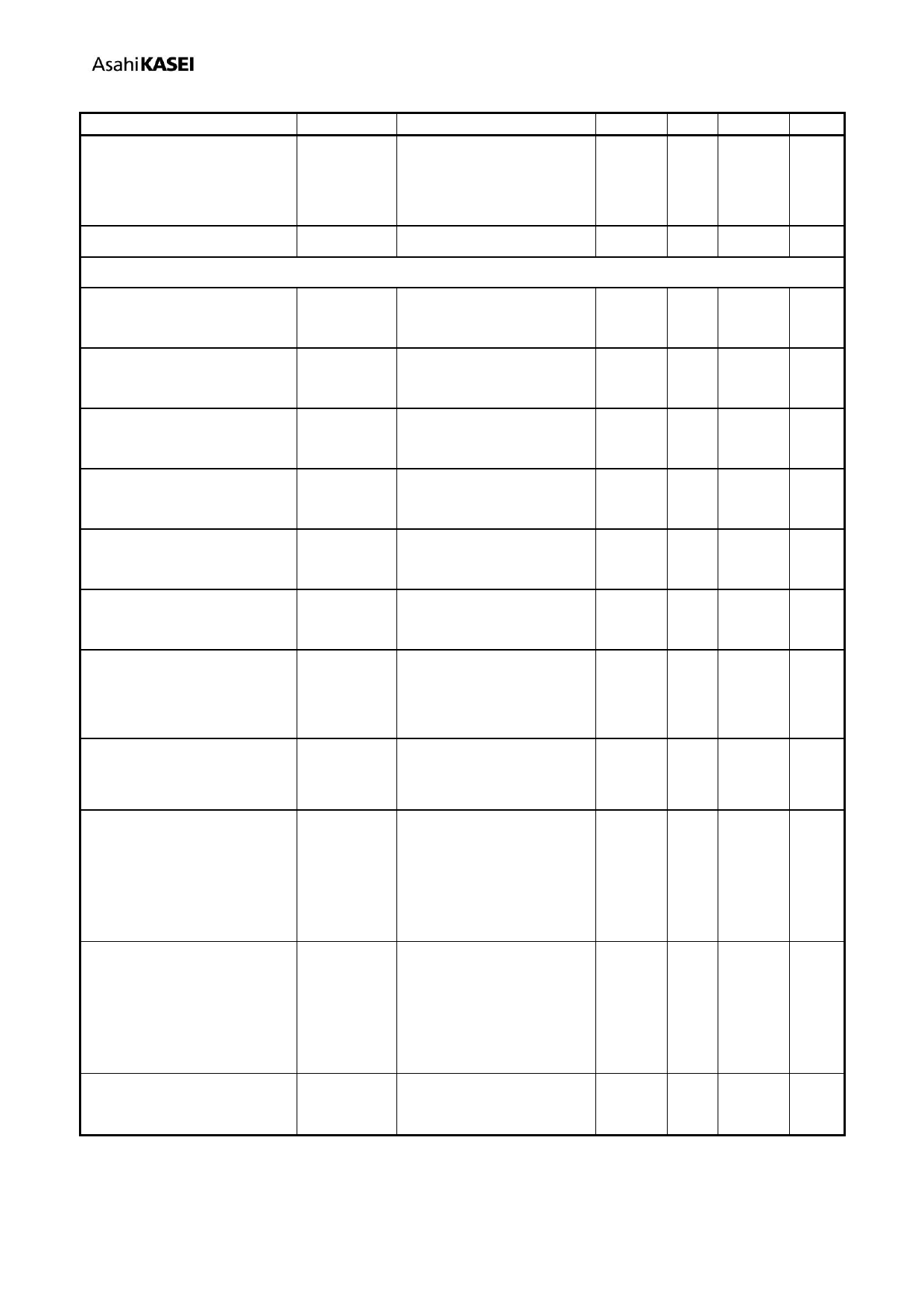
[AP1014AEC]
Parameter
Driver on resistance
(High side + Low side)
(Note 4)
Symbol
Condition
RON3
Design
certification
Iload=0.7A, Ta=85℃
Min. Typ. Max. Unit
- 0.48 0.72 Ω
Body diode forward voltage
VFMD
IF=100mA
-
0.8 1.2
V
Control logic
Input High level voltage
(INnA, INnB, SEL and EN)
VIH
VC=2.7V~5.5V
0.7×VC -
-
V
Input Low level voltage
VIL
(INnA, INnB, SEL and EN)
-
- 0.3×VC V
Input High level current
(SEL and EN)
IIH
VIH=3.0V
9
15 21 μA
Input Low level current
(INnA and INnB)
IIL
VIL=0V
-1.0
-
-
μA
Input pulse rize time
(INnA and INnB)
tr
VC=2.7V~5.5V
-
-
1.0
μs
Input pulse fall time
tf
(INnA and INnB)
-
-
1.0
μs
H-Bridge propagation delay
time
(INnB=”L”→OUTnA=”H”)
tPDLH
1k Load between
OUTnA and OUTnB.
SEL=”L”, NnA = “H”,
INnB = 200kHz
-
-
0.5
μs
H-Bridge propagation delay
time
(INnB=”H”→OUTnA=”L”)
tPDHL
-
-
0.5
μs
10 Load between
OUTnA/B and GND.
H-Bridge propagation delay
time (Hi-Z→”H”) (Note 4)
tPDZH
10 Load between
OUTnA/B and VM.
-
-
0.5
μs
Time to change from 50%
to 75%
10 Load between
OUTnA/B and GND.
H-Bridge propagation delay
time (Hi-Z→”L”) (Note 4)
tPDZL
10 Load between
OUTnA/B and VM.
-
Time to change from 50%
to 25%
-
0.5
μs
H-bridge output pulse width
20 Load between OUTA
tPW and OUTB. input pluse
0.7
-
1.5
μs
(Note 4)
width : 1s
Note 4. Not tested in production.
MS1548-E-00
-8-
2014/03
Share Link: 