AMS2263 View Datasheet(PDF) - Advanced Monolithic Systems Inc
Part Name
Description
Manufacturer
AMS2263 Datasheet PDF : 12 Pages
| |||
AMS 2263
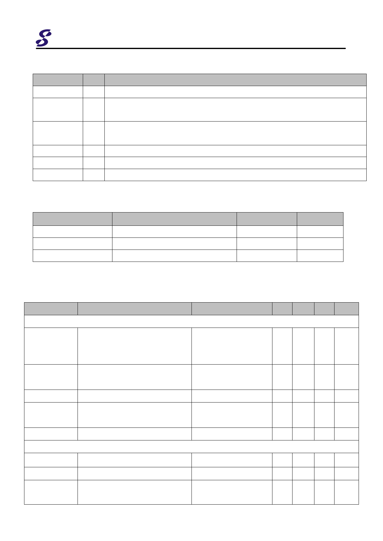
TERMINAL ASSIGNMENTS
Pin Name
GND
FB
RI
SENSE
VDD
GATE
I/O
Description
P Ground
I
Feedback input pin. The PWM duty cycle is determined by voltage level into this pin
and SENSE pin input.
I
Internal Oscillator frequency setting pin. A resistor connected between RI and GND
sets the PWM frequency.
I
Current sense input pin. Connected to MOSFET current sensing resistor node.
P Chip DC power supply pin.
O Totem-pole gate drive output for the power MOSFET.
RECOMMENDED OPERATING CONDITION
Symbol
Parameter
VDD
RI
TA
VDD Supply Voltage
RI Resistor Value
Operating Ambient Temperature
Min - Max
10 to 30
100
-20 to 85
Unit
V
Kohm
oC
ELECTRICAL CHARACTERISTICS
(TA = 25OC if not otherwise noted)
Symbol
Parameter
Supply Voltage (VDD)
I_VDD_Startup VDD Start up
Current
I_VDD_Ops
Operation Current
UVLO(ON)
VDD Under Voltage Lockout Enter
UVLO(OFF) VDD Under Voltage Lockout Exit
(Recovery)
VDD_Clamp VDD Zener Clamp Voltage
Feedback Input Section(FB Pin)
AVCS
PWM Input Gain
VFB_Open
IFB_Short
VFB Open Loop Voltage
FB pin short circuit current
Test Conditions
VDD =12.5V, RI=100K
Measure Leakage
current into VDD
VDD=16V,
RI=100Kohm, VFB=3V
IVDD = 5 mA
ΔVFB /ΔVcs
Short FB pin to GND
and measure current
Min Typ Max Unit
3
20 uA
1.4
mA
7.5 8.5 9.5 V
13.5 14.5 15.5 V
34
V
2.0
V/V
4.8
V
1
mA
4
Advanced Monolithic Systems http://www.ams-semitech.com
Share Link: 