SD500N(1994) View Datasheet(PDF) - International Rectifier
Part Name
Description
Manufacturer
SD500N Datasheet PDF : 6 Pages
| |||
SD500N/R Series
Bulletin I2095 rev. A 08/94
Thermal and Mechanical Specifications
Parameter
T
J
Tstg
RthJC
RthCS
T
wt
Max. junction operating temperature range
Max. storage temperature range
Max. thermal resistance, junction to case
Max. thermal resistance, case
to heatsink
Max. allowed mounting torque ±10%
Approximate weight
Case style
SD500N/R
-40 to 150
-55 to 200
0.1
0.04
50
454
B-8
Units Conditions
°C
K/W
Nm
g
DC operation
Mounting surface, smooth, flat and
greased
Not lubricated threads
See Outline Table
∆RthJC Conduction
(The following table shows the increment of thermal resistence RthJC when devices operate at different conduction angles than DC)
Conduction angle Sinusoidal conduction Rectangular conduction Units Conditions
180°
120°
90°
60°
30°
0.012
0.014
0.017
0.025
0.042
0.008
0.014
0.019
0.026
0.042
K/W
TJ = TJ max.
Ordering Information Table
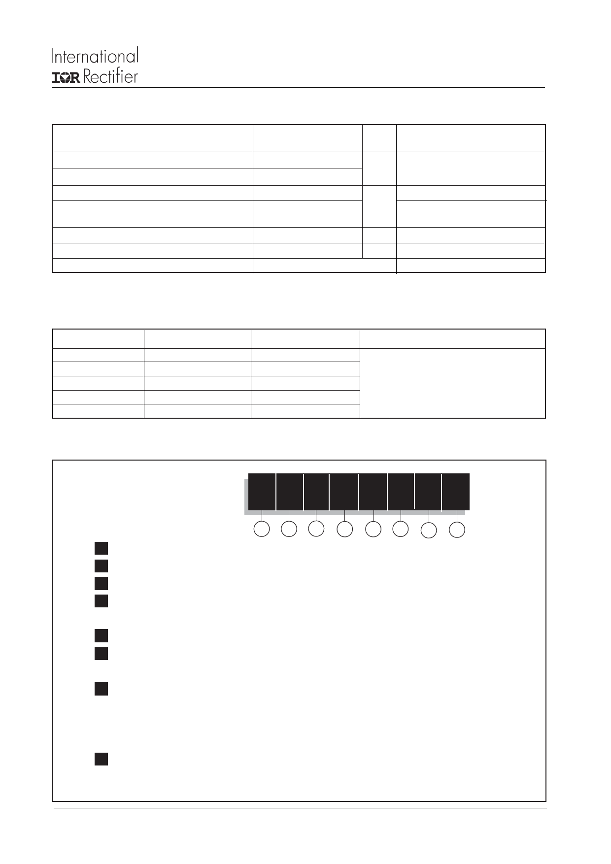
Device Code
SD 50 0 N 45 P S C
123 4 567 8
1 - Diode
2 - Essential part number
3 - 0 = Standard recovery
4 - N = Stud Normal Polarity (Cathode to Stud)
R = Stud Reverse Polarity (Anode to Stud)
5 - Voltage code: Code x 100 = VRRM (See Voltage Ratings table)
6 - P = Stud base B-8 3/4" 16UNF-2A
M = Stud base B-8 M24 X 1.5
7 - S = Isolated lead with silicone sleeve
(Red = Reverse Polarity; Blue = Normal Polarity)
T = Threaded Top Terminal 3/8" 24UNF-2A
None = Non isolated lead
8 - C = Ceramic Housing
NOTE: Available for rotating applications (Contact factory)
www.irf.com
3
Share Link: 