BU1425AK View Datasheet(PDF) - ROHM Semiconductor
Part Name
Description
Manufacturer
BU1425AK Datasheet PDF : 32 Pages
| |||
Multimedia ICs
BU1425AK / BU1425AKV
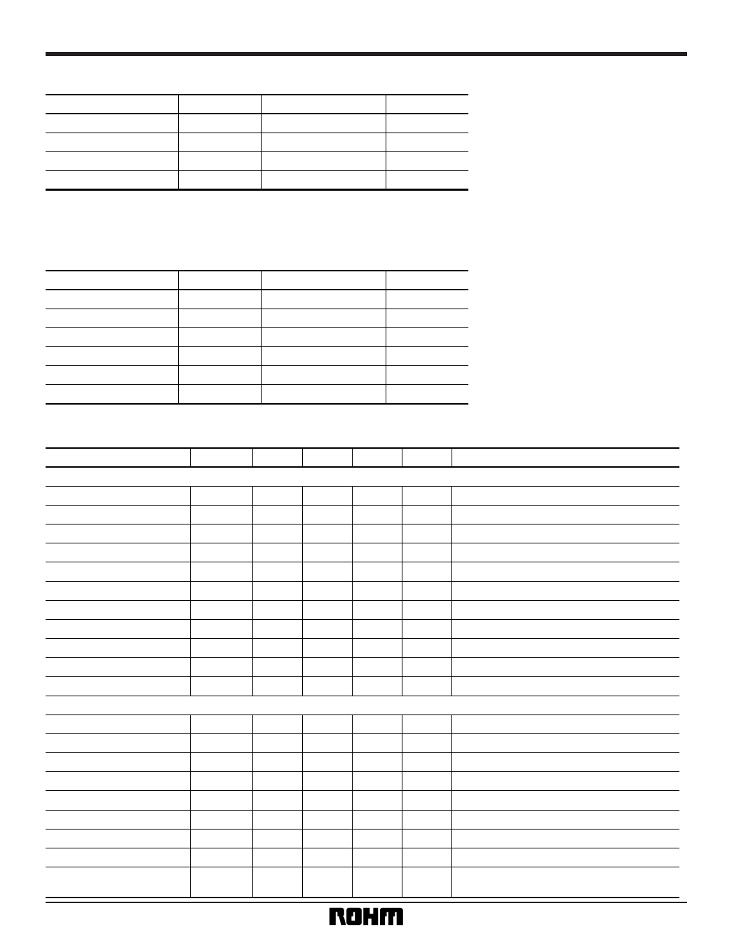
•Absolute maximum ratings (Ta = 25°C)
Parameter
Symbol
Limits
Unit
Applied voltage
VDD, AVDD
– 0.5 ~ + 7.0
V
Input voltage
VIN
– 0.3 ~ IOVDD + 0.3
V
Storage temperature
Tstg
– 55 ~ + 150
Power dissipation
Pd
1350∗1
∗1 Reduced by 11mW for each increase in Ta of 1°C over 25°C.
∗1 When mounted on 120mm × 140mm × 1.0mm glass epoxy board.
∗ Operation is not guaranteed at this value.
᭺ Not designed for radiation resistance.
•Recommended operating conditions
°C
mW
Parameter
Power supply voltage
Power supply voltage
Input high level voltage
Symbol
VDD = AVDD∗
IOVDD
VIH
Limits
4.50 ~ 5.50
3.30 ~ 5.50
2.1 ~ VDD
Unit
V
V
V
Input low level voltage
VIL
0 ~ + 0.8
V
Analog input voltage
VAIN
0 ~ AVDD
V
Operating temperature
Topr
– 25 ~ + 60
°C
∗ Should be used at VDD = AVDD.
•Electrical characteristics (unless otherwise noted, Ta = 25°C, VDD = AVDD = 5.0V, GND = AVSS = VGND = CGND = YGND)
Parameter
Symbol Min.
Typ.
Max.
Unit
Conditions
〈Digital block〉
Burst frequency 1
fBST1
— 3.57954 —
MHz
Burst frequency 2
fBST2
— 4.43361 —
MHz
Burst cycle
CBST
—
9
—
CYC
Operating circuit current 1
Idd1
—
80
—
mA 27MHz color bar
Operating circuit current 2
Idd2
—
40
—
mA 27MHz color bar PD mode
Output high level voltage
VOH
4.0
4.5
—
V
IOH = – 2.0mA
Output low level voltage
VOL
—
0.5
1.0
V
IOH = 2.0mA
Input high level voltage
VIH
2.1
—
—
V
Input low level voltage
VIL
—
—
0.8
V
Input high level current
IIH
– 10
0.0
10.0
µA
Input low level current
IIL
– 10
0.0
10.0
µA
〈DAC block〉
DAC resolution
RES
—
9
—
BITS
Linearity error
EL
— ± 0.5 ± 3.0
LSB IR = 1.2kΩ
Y white level current
IYW
—
25.14
—
mA
Y black level current
IYB
—
7.24
—
mA
Y zero level current
IYZ
– 10
0.0
10.0
µA
V white level current
IYW
—
25.14
—
mA
V black level current
IYB
—
7.24
—
mA
V zero level current
Sleep mode current
IYZ
Iddpd
– 10
—
0.0
10.0
µA
—
1.0
µA
VIN Max. = IOVDD + 0.3V
VIN Min. = – 0.3V
4
Share Link: 