MM74C165 View Datasheet(PDF) - Fairchild Semiconductor
Part Name
Description
Manufacturer
MM74C165 Datasheet PDF : 6 Pages
| |||
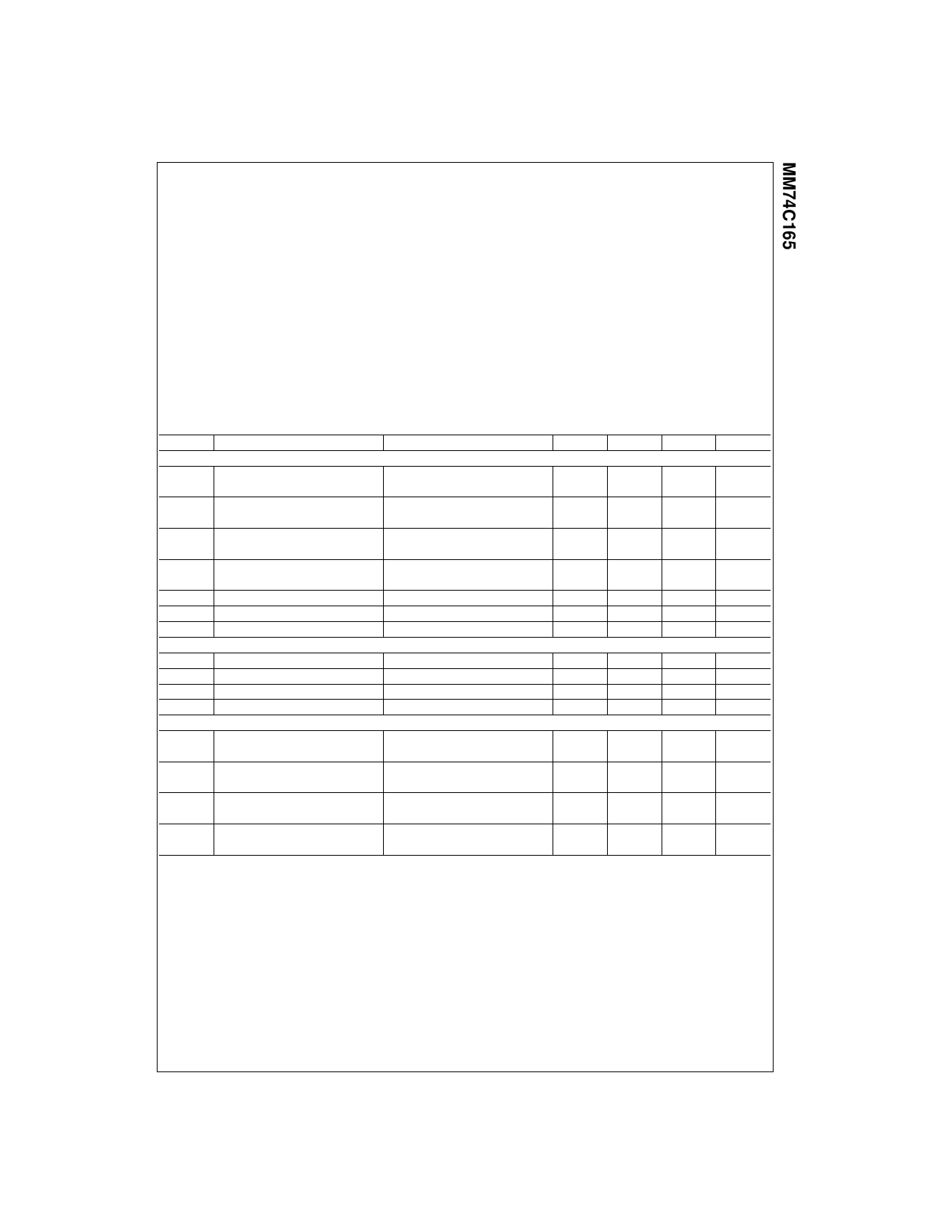
Absolute Maximum Ratings(Note 1)
Voltage at Any Pin
Operating Temperature Range
Storage Temperature Range
Absolute Maximum VCC
Power Dissipation
Dual-In-Line
Small Outline
Operating VCC Range
Lead Temperature
(Soldering, 10 seconds)
−0.3V to VCC + 0.3V
−55°C to +125°C
−65°C to +150°C
18V
700 mW
500 mW
3V to 15V
260°C
Note 1: “Absolute Maximum Ratings” are those values beyond which the
safety of the device cannot be guaranteed. Except for “Operating Tempera-
ture Range” they are not meant to imply that the devices should be oper-
ated at these limits. The Electrical Characteristics table provides conditions
for actual device operation.
DC Electrical Characteristics
Min/Max limits apply across temperature range unless otherwise noted
Symbol
Parameter
Conditions
CMOS TO CMOS
VIN(1)
Logical “1” Input Voltage
VIN(0)
Logical “0” Input Voltage
VOUT(1)
Logical “1” Output Voltage
VOUT(0)
Logical “0” Output Voltage
IIN(1)
Logical “1” Input Current
IIN(0)
Logical “0” Input Current
ICC
Supply Current
CMOS TO LPTTL INTERFACE
VCC = 5V
VCC = 10V
VCC = 5V
VCC = 10V
VCC = 5V, IO = −10 µA
VCC = 10V, IO = −10 µA
VCC = 5V, IO = +10 µA
VCC = 10V, IO = +10 µA
VCC = 15V, VIN = 15V
VCC = 15V, VIN = 0V
VCC = 15V
VIN(1)
Logical “1” Input Voltage
VCC = 4.75V
VIN(0)
Logical “0” Input Voltage
VCC = 4.75V
VOUT(1)
Logical “1” Output Voltage
VCC = 4.75V, IO = −360 µA
VOUT(0)
Logical “0” Output Voltage
VCC = 4.75V, IO = 360 µA
OUTPUT DRIVE (See Family Characteristics Data Sheet) (short circuit current)
ISOURCE
ISOURCE
ISINK
ISINK
Output Source Current
(P-Channel)
Output Source Current
(P-Channel)
Output Sink Current
(N-Channel)
Output Sink Current
(N-Channel)
VCC = 5V
TA = 25°C, VOUT = 0V
VCC = 10V
TA = 25°C, VOUT = 0V
VCC = 5V
TA = 25°C, VOUT = VCC
VCC = 10V
TA = 25°C, VOUT = VCC
Min
Typ
Max
3.5
8.0
1.5
2.0
4.5
9.0
0.5
1.0
0.005
1.0
−1.0
−0.005
0.05
300
VCC − 1.5
0.8
2.4
0.4
−1.75
−8.0
1.75
8.0
−3.3
−15
3.6
16
Units
V
V
V
V
µA
µA
µA
V
V
V
V
mA
mA
mA
mA
3
www.fairchildsemi.com
Share Link: 