CXA3275Q View Datasheet(PDF) - Sony Semiconductor
Part Name
Description
Manufacturer
CXA3275Q Datasheet PDF : 22 Pages
| |||
CXA3275Q
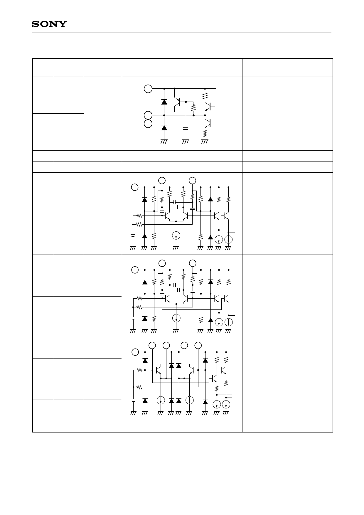
Pin Description and Equivalent Circuit
Pin
No.
Symbol
Pin voltage
[V]
Equivalent circuit
1 IFOUT1
IFVcc
3
40k
2.5
1
2
2 IFOUT2
Description
IF outputs.
IFOUT1 and IFOUT2 output a
balanced signal.
When taking a signal as an
unbalanced output, connect
the pin not used for output to
IFVCC. At this time the output
stage current is saved.
3 IFVcc
—
4 IFGND
—
5 VLOSC2
2.5
5
19
20k
6
20k
IF amplifier power supply.
IF amplifier GND.
Vcc
6 VLOSC1
2.5
3k
3k
20k
20k
External resonance circuit
connection for VL oscillator.
7 VHOSC2
2.5
8 VHOSC1
2.5
7
19
20k
3k
3k
20k
8
20k
20k
Vcc
External resonance circuit
connection for VH oscillator.
9
UOSCB2
UHF: 2.2
VL/VH: 2.3
10
UOSCE2
UHF: 1.5
VL/VH: –
11
UOSCE1
UHF: 1.5
VL/VH: –
12
UOSCB1
UHF: 2.2
VL/VH: 2.3
13 RFGND
—
9 10
19
3k
11 12
3k
Vcc
External resonance circuit
connection for UHF oscillator.
Analog GND.
–3–
Share Link: 