LT1055MHPBF(Rev_D) View Datasheet(PDF) - Linear Technology
Part Name
Description
Manufacturer
LT1055MHPBF Datasheet PDF : 20 Pages
| |||
LT1055/LT1056
ELECTRICAL CHARACTERISTICS
For MIL-STD components, please refer to LTC883 data sheet for test
listing and parameters.
Note 1: Stresses beyond those listed under Absolute Maximum Ratings
may cause permanent damage to the device. Exposure to any Absolute
Maximum Rating condition for extended periods may affect device
reliability and lifetime.
Note 2: Offset voltage is measured under two different conditions:
(a) approximately 0.5 seconds after application of power; (b) at TA = 25°C
only, with the chip heated to approximately 38°C for the LT1055 and to
45°C for the LT1056, to account for chip temperature rise when the device
is fully warmed up.
Note 3: 10Hz noise voltage density is sample tested on every lot of A
grades. Devices 100% tested at 10Hz are available on request.
Note 4: This parameter is tested on a sample basis only.
Note 5: Current noise is calculated from the formula: in = (2qlB)1/2, where
q = 1.6 • 10–19 coulomb. The noise of source resistors up to 1GΩ swamps
the contribution of current noise.
Note 6: Offset voltage drift with temperature is practically unchanged when
the offset voltage is trimmed to zero with a 100k potentiometer between
the balance terminals and the wiper tied to V+. Devices tested to tighter
drift specifications are available on request.
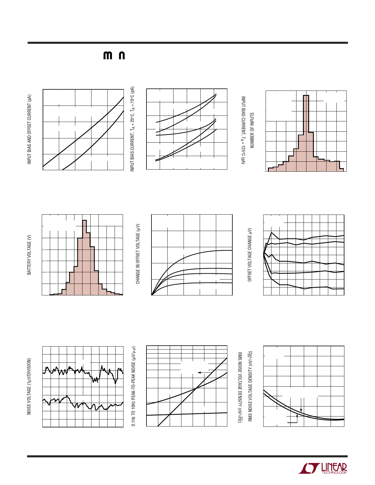
TYPICAL PERFORMANCE CHARACTERISTICS
Input Bias and Offset Currents
vs Temperature
1000
300
VS = ±15V
VCM = 0V
WARMED UP
BIAS OR OFFSET CURRENTS
MAY BE POSITIVE OR NEGATIVE
100
BIAS CURRENT
30
10
3
0
OFFSET CURRENT
25
50
75 100 125
AMBIENT TEMPERATURE (°C)
LT1055/56 G01
Input Bias Current Over the
Common Mode Range
120
VS = ±15V
WARMED UP
80
TA = 125°C
40
A
TA = 70°C
1200
800
400
0
A
TA = 25°C
0
– 40
– 80
–120
–15
TA = 70°C
TA = 125°C
– 400
B
– 800
A = POSITIVE INPUT CURRENT
B
B = NEGATIVE INPUT CURRENT
–1200
–10 –5
0
5
10 15
COMMON MODE INPUT VOLTAGE (V)
LT1055/56 G02
Distribution of Offset Voltage Drift
with Temperature (H Package)*
140 VS = ±15V
120
634 UNITS TESTED
FROM THREE RUNS
50% TO
±1.5µV/ °C
100
80
60
40
20
0
–10 –8 –6 –4 –2 0 2 4 6 8 10
OFFSET VOLTAGE DRIFT WITH TEMPERATURE (µV/°C)
*DISTRIBUTION IN THE PLASTIC (N8) PACKAGE
IS SIGNIFICANTLY WIDER.
LT1055/56 G04
Warm-Up Drift
100
VS = ±15V
TA = 25°C
80
60
LT1056CN8
40
LT1055CN8
20
LT1056 H PACKAGE
LT1055 H PACKAGE
0
0
1
2
3
4
5
TIME AFTER POWER ON (MINUTES)
LT1055/56 G05
Distribution of Input Offset
Voltage (N8 Package)
160 VS = ±15V
140
TA = 25°C
550 UNITS
120
TESTED FROM
TWO RUNS
100 (LT1056)
50% YIELD
TO ±140µV
80
60
40
20
0
–800 –600 –400 –200 0 200 400 600 800
INPUT OFFSET VOLTAGE (µV)
LT1055/56 G03
Long Term Drift of
Representative Units
50
40
VS = ±15V
TA = 25°C
30
20
10
0
–10
–20
–30
–40
–50
0
1
2
3
TIME (MONTHS)
4
5
LT1055/56 GO6
10556fd
6
For more information www.linear.com/LT1055
Share Link: 