TS922 View Datasheet(PDF) - STMicroelectronics
Part Name
Description
Manufacturer
TS922 Datasheet PDF : 24 Pages
| |||
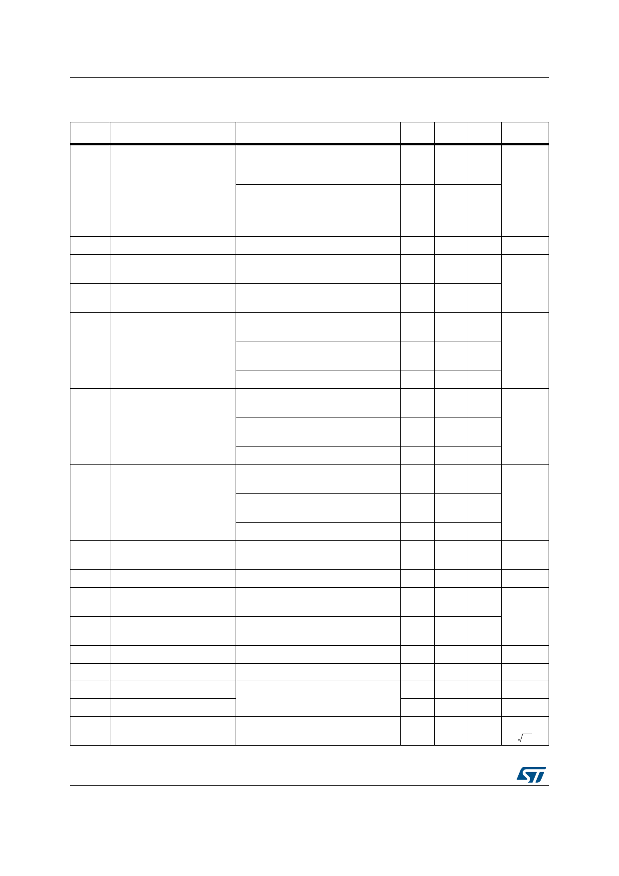
Electrical characteristics
TS922, TS922A
Table 4. Electrical characteristics measured at VCC = 5 V, VCC- = 0 V, Vicm = VCC/2,
Tamb = 25 °C, and RL connected to VCC/2 (unless otherwise specified)
Symbol
Parameter
Conditions
Min. Typ. Max. Unit
Vio Input offset voltage
TS922
TS922A
TS922IJ (Flip-chip)
Tmin ≤ Tamb ≤ Tmax
TS922
TS922A
TS922IJ (Flip-chip)
ΔVio/ΔT Input offset voltage drift
Iio Input offset current
Vout = VCC/2
Tmin ≤ Tamb ≤ Tmax
Iib Input bias current
Vout = VCC/2
Tmin ≤ Tamb ≤ Tmax
RL= 10 kΩ
Tmin ≤ Tamb ≤ Tmax
VOH High level output voltage
RL = 600 Ω
Tmin ≤ Tamb ≤ Tmax
RL = 32 Ω
RL= 10 kΩ
Tmin ≤ Tamb ≤ Tmax
VOL Low level output voltage
RL = 600 Ω
Tmin ≤ Tamb ≤ Tmax
RL = 32 Ω
RL= 10 kΩ, Vout = 2 Vp-p
Tmin ≤ Tamb ≤ Tmax
Avd Large signal voltage gain
RL = 600 Ω, Vout = 2 Vp-p
Tmin ≤ Tamb ≤ Tmax
RL = 32 Ω, Vout = 2 Vp-p
Icc Total supply current
No load, Vout = VCC/2
Tmin ≤ Tamb ≤ Tmax
GBP Gain bandwidth product
RL = 600 Ω
CMR
Common mode rejection
ratio
Vicm = 0 to 5 V
Tmin ≤ Tamb ≤ Tmax
SVR
Supply voltage rejection ratio
VCC = 4.5 to 5.5 V
Tmin ≤ Tamb ≤ Tmax
Io Output short-circuit current
SR Slew rate
φm Phase margin at unit gain
Gm Gain margin
en
Equivalent input noise
voltage
RL = 600 Ω, CL =100 pF
f = 1 kHz
3
0.9
1.5
mV
5
1.8
2.5
2
μV/°C
1
30
30
nA
15 100
100
4.9
4.9
4.85
V
4.85
4.4
50
50
120
mV
120
300
200
70
35
20
V/mV
16
2
3
3.2
mA
4
MHz
60 80
56
dB
60 85
60
50 80
mA
0.7 1.3
68
V/μs
Degrees
12
dB
9
--n----V-----
Hz
8/24
DocID5150 Rev 11
Share Link: 