MU9C1965L-12TCC View Datasheet(PDF) - Music Semiconductors
Part Name
Description
Manufacturer
MU9C1965L-12TCC Datasheet PDF : 28 Pages
| |||
MU9C1965A/L LANCAM® MP
PIN DESCRIPTIONS Continued
/MI (Match Input, Input, TTL)
The /MI input prioritizes devices in vertically cascaded
systems. It is connected to the /MF output of the previous
device in the daisy chain. The /MI pin on the first device in
the chain must be tied HIGH.
/FI (Full Input, Input, TTL)
The /FI input generates a CAM-Memory-System-Full
indication in vertically cascaded systems. It is connected
to the /FF output of the previous device in the daisy chain.
The /FI pin on the first device in a chain must be tied LOW.
/MA (Device Match Flag, Output, TTL)
The /MA output is LOW when one or more valid matches
occur during the current or the last previous compare cycle.
The /MA output is not qualified by /EC or /MI, and reflects
the match flag from that specific device’s Status register.
/MA will be reset when the active register set is changed.
/RESET (Reset, Input, TTL)
/RESET must be driven LOW to place the device in a known
state before operation, which will reset the device to the
conditions shown in Table 5 on page 10. The /RESET pin
should be driven by TTL levels, not directly by an RC
timeout. /E must be kept HIGH during /RESET.
/MM (Device Multiple Match Flag, Output, TTL)
The /MM output is LOW when more than one valid match
occurs during the current or the last previous compare cycle.
The /MM output is not qualified by /EC or /MI, and reflects
the Multiple Match flag from that specific device’s Status
register. /MM will be reset when the active register set is
changed.
/FF (Full Flag, Output, TTL)
If enabled in the Control register, the /FF output goes LOW
when no empty memory locations exist within the device
(and in the daisy chain above the device as indicated by
the /FI pin). The System Full flag is the /FF pin of the last
device in the daisy chain, and the Next Free address resides
in the device with /FI LOW and /FF HIGH. If disabled in the
Control register, the /FF output only depends on the /FI
input (/FF = /FI).
TEST1, TEST2 (Test, Input, TTL)
These pins enable MUSIC production test modes that are
not usable in an application. They should be connected to
ground, either directly or through a pull-down resistor, or
they may be left unconnected. These pins may not be
implemented on all versions of this product.
VCC, GND (Positive Power Supply, Ground)
These pins are the power supply connections to the
LANCAM MP. VCC must meet the voltage supply
requirements in the Operating Conditions section relative
to the GND pins, which are at 0 Volts (system reference
potential), for correct operation of the device. All the
ground and power pins must be connected to their
respective planes with adequate bulk and high frequency
bypassing capacitors in close proximity to the device.
Note: -90 or slower switching characteristics can be
operated without the GND connections on pins 1, 2, 20, 21,
22, 41, 42, 60, 61, and 62. MUSIC, however, recommends the
usage of these GND connections to ensure full compatibility
with future products.
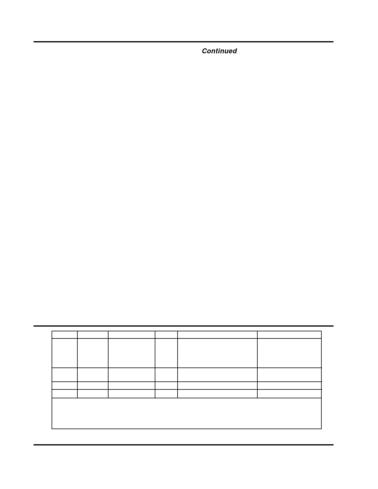
/W
LOW
HIGH
LOW
HIGH
/CM
LOW
LOW
HIGH
HIGH
Cycle Type
Command write
Command read
TCO 2nd cycle
Data write
Data read
“f” Bit
0
1
0
1
X
X
X
X
DQ31–16
Non-TCO Instruction
Non-TCO Instruction
TCO Instruction (Read register)*
TCO Instruction (Write register)
Status Register bits 31–16
Status Register bits 31‚Äì16‚ÄÝ
Data to CR, MRX, Mem.
Data from CR, MRX, Mem.
DQ15–0
XXXX
Absolute Address
XXXX
Value to Register
Status Register bits 15–0
Register contents*
Data to CR, MRX, Mem.
Data from CR, MRX, Mem.
Notes:
* A CW of a TCO Instruction with the “f” bit set to 0 sets up a Register read in the following cycle. The
following cycle must be a Command Read cycle, otherwise the register read will be cancelled.
‚ÄÝ Upper 16 bits will be Status Register bits 31‚Äì16, except for a read of the Page Address register, in which
case they will be all zeros.
Table 3: DQ Bus Multiplexing
Rev. 1a
4
Share Link: 