LTC1531CSW View Datasheet(PDF) - Linear Technology
Part Name
Description
Manufacturer
LTC1531CSW Datasheet PDF : 16 Pages
| |||
LTC1531
APPLICATIONS INFORMATION
VPW
VPW
21k
VGP
2k
VREG
23k
16k
1
ISOGND
16k
1
ISOGND
1531 F05
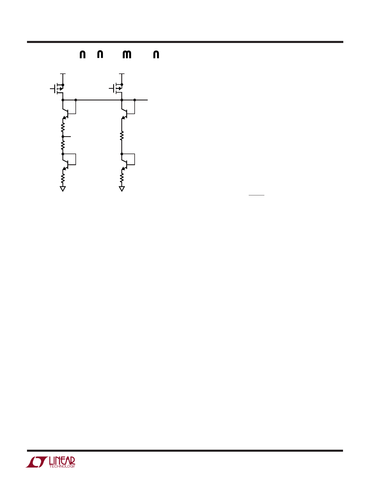
Figure 5. VREG Output Stage
V3 ≠ V4, the input impedance due to leakage currents is
about 15MΩ to 20MΩ. Since the comparator is turned on
only for the last 10µs of the 108µs VREG period, the charge
injection occurs at about the 98µs point with a coupling
capacitance of 2pF per input.
The CMPOUT signal is typically used to provide hyster-
esis, as in the Isolated Temperature Control application.
CMPOUT is the latched result of the previous comparison
and is active during the following VREG ON period. CMPOUT
is powered by VREG, the internal 2.5V regulated output,
and is in high impedance except during the 108µs
VREG ON time. When active, CMPOUT is switched low to
ISOGND or high to VREG depending on the stored result of
the previous comparison. The stored CMPOUT data is
reset during power-up. CMPOUT is not necessarily reset
by the powered side SHDN pin, except when shutdown
results in VPW drooping low enough to trigger a power-on
reset on the isolated side between 1.5V to 2.5V.
tance, which will subsequently be discharged between
samples, will consume power from VPW.
ISOLATED COMPARATOR INPUTS AND CMPOUT
The LTC1531 isolated comparator has a 4-input
summing comparator that performs the following
comparison:
(V1 + V2)/2 > (V3 + V4)/2
By rearranging the equation, for example, a dual differen-
tial comparison is performed:
(V1 – V4) > (V3 – V2) or (V1 – V3) > (V4 – V2)
The input has a rail-to-rail input and common mode
voltage range of VPW-ISOGND. The summing nature of the
inputs allows midsupply referencing. For example, con-
necting V3 to VREG and V4 to ISOGND sums together to
provide VREG/2 for the negative comparator input. See for
example, the Isolated Switch Control.
Charge injection and leakage currents occur at the com-
parator inputs. The amount depends on how the compara-
tor is used. Minimum leakage currents occur with V1 = V2
and V3 = V4 where the input impedance is from charge
injection and is nominally 300MΩ. When V1 ≠ V2 or
DATA, VALID, ZCDATA
During a power cycle, the VALID signal goes high if a valid
comparison was made during the previous listen cycle.
VALID goes low at the beginning of the next listen cycle.
The low-to-high transition of VALID can be used to clock
DATA into external circuitry. VALID is delayed 200ns after
the DATA output. In order for a comparison to occur,
sufficient power must be stored on the isolated side
storage capacitor.
The DATA output holds the last received compare result.
DATA is reset to zero on power-up and shutdown. The
VALID output is held high for one power cycle following a
correctly received compare result. The received DATA
value from the isolated side contains redundancy to im-
prove noise immunity.
The ZCDATA is a 25µs output pulse triggered by the zero-
cross comparator. In order for a pulse to occur, the DATA
output must be at logic 1 and the ZCPOS-ZCNEG zero-
cross comparator input crosses 0V after the input has
exceeded the ±150mV to 800mV of hysteresis. The zero-
cross comparator output is typically used to trigger a triac
from a 60Hz RC phase shifted AC line signal. See Typical
Applications.
7
Share Link: 