TC74A0-5.0VCT View Datasheet(PDF) - Microchip Technology
Part Name
Description
Manufacturer
TC74A0-5.0VCT Datasheet PDF : 16 Pages
| |||
TC74
1.0 ELECTRICAL
CHARACTERISTICS
Absolute Maximum Ratings*
Supply Voltage (VDD) ............................................ +6V
Voltage On Any Pin ....... (GND – 0.3V) to (VDD + 0.3V)
Current On Any Pin .......................................... ±50 mA
Operating Temperature (TA)........................ See Below
Storage Temperature (TSTG) .............. -65°C to +150°C
*Stresses above those listed under "Absolute Maximum Rat-
ings" may cause permanent damage to the device. These are
stress ratings only and functional operation of the device at
these or any other conditions above those indicated in the
operation sections of the specifications is not implied. Expo-
sure to Absolute Maximum Rating conditions for extended
periods may affect device reliability.
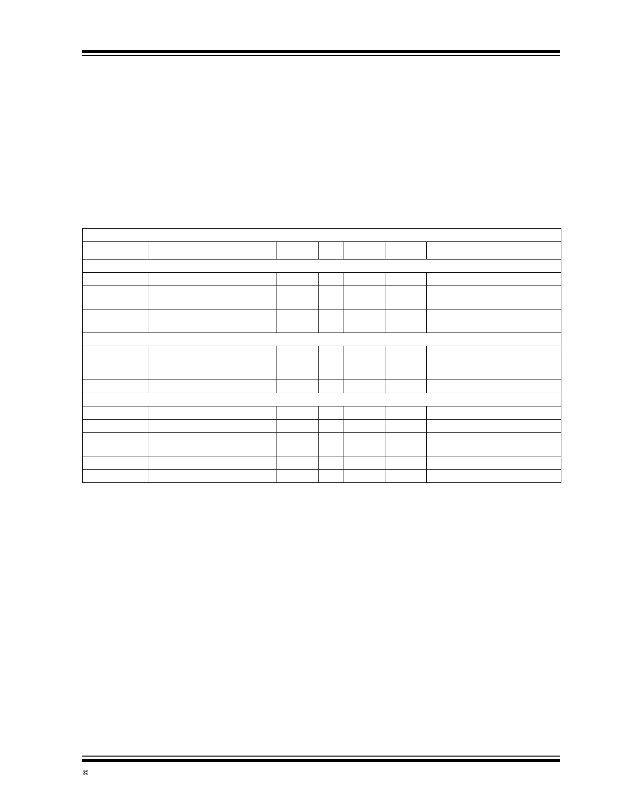
TC74 ELECTRICAL SPECIFICATIONS
Electrical Characteristics: VDD = 3.3V or 5.0V (Note 5), -40°C ≤ TA ≤ 125°C, unless otherwise noted.
Symbol
Parameter
Min Typ. Max
Unit
Test Conditions
Power Supply
VPOR
IDD
Power-on Reset Threshold
Operating Current
1.2
—
2.2
—
200 350
V
VDD Falling Edge or Rising Edge
µA VDD = 5.5V
Serial Port Inactive (Note 1)
IDD-STANDBY
Standby Supply Current
—
5
10
µA VDD = 3.3V
Serial Port Inactive (Note 1)
Temperature to Bits Converter
TERR
CR
Temperature Accuracy TC74A
Conversion Rate
-2
—
+2
-3
—
—
+2
4
8
—
°C +25°C <TA < +85°C
0°C < TA < +125°C
-40°C < TA < 0°C
Sps (Note 2)
Serial Port Interface
VIH
Logic Input High
0.8 x VDD —
—
V
VIL
Logic Input Low
—
— 0.2 x VDD
V
VOL
SDA Output Low
—
—
0.4
—
—
0.6
V
IOL = 3 mA
V
IOL = 6 mA (Note 3)
CIN
Input Capacitance SDA, SCL
—
5
—
pF
ILEAK
I/O Leakage
-1
0.1
1
µA
Note 1: Operating current is an average value integrated over multiple conversion cycles. Transient current may exceed this specification.
2: Maximum ensured conversion time after Power-on Reset (POR to DATA_RDY) is 250 msec.
3: Output current should be minimized for best temperature accuracy. Power dissipation within the TC74 will cause self-heating and
temperature drift error.
4: SDA and SCLK must be connected to VDD or GND.
5: VDD = 3.3V for TC74X -3.3VCT. VDD = 5.0V for TC74X -5.0VCT. All part types of the TC74 will operate properly over the wider power
supply range of 2.7V to 5.5V. Each part type is tested and specified for rated accuracy at its nominal supply voltage. As VDD varies from
the nominal value, accuracy will degrade 1°C/V of VDD change.
© 2002 Microchip Technology Inc.
DS21462B-page 3
Share Link: 