ADIS16209CCCZ(Rev0) View Datasheet(PDF) - Analog Devices
Part Name
Description
Manufacturer
ADIS16209CCCZ
(Rev.:Rev0)
(Rev.:Rev0)
Analog Devices
ADIS16209CCCZ Datasheet PDF : 16 Pages
| |||
Digital I/O Lines
The ADIS16209 provides two, general purpose, digital
input/output lines that have several configuration options.
Table 11. Digital I/O Line Configuration Registers
Function
[Priority] Register
Data-Ready I/O Indicator
[1]
MSC_CTRL
Alarm Indicator
[2]
ALM_CTRL
General-Purpose I/O Configuration [3]
GPIO_CTRL
General-Purpose I/O Line Communication
GPIO_CTRL
Data-Ready I/O Indicator
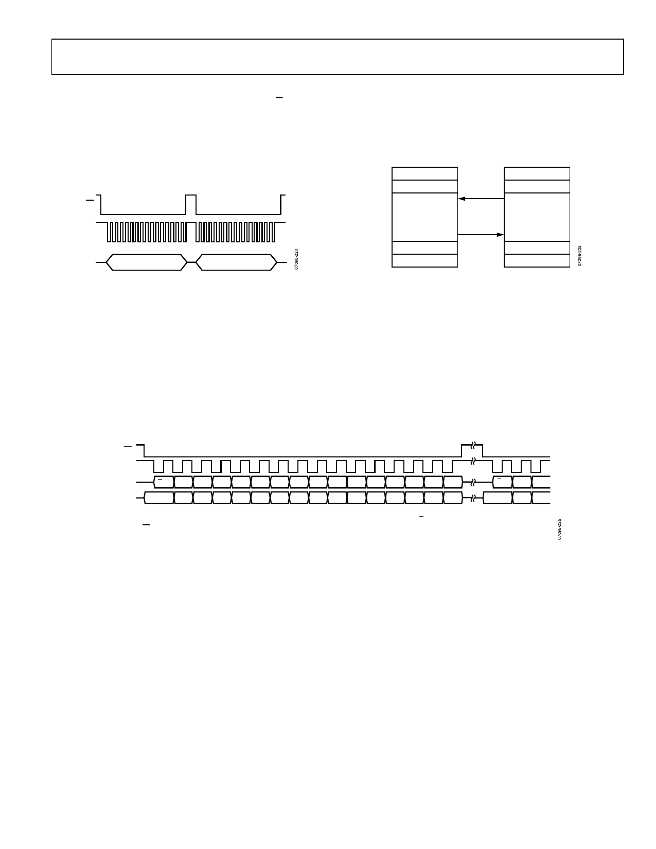
The MSC_CTRL register provides controls for a data-ready
function. For example, writing 0x05 to this register enables this
function and establishes DIO2 as an active-low, data-ready line.
The duty cycle is 25% (±10% tolerance).
Table 12. MSC_CTRL Bit Descriptions
Bit Description
(Default = 0x0000)
15:11 Not used
10
Self-test at power-on: 1 = disabled, 0 = enabled
9
Not used
8
Self-test enable (temporary, bit is volatile)
1 = enabled, 0 = disabled
7:3 Not used
2
Data-ready enable: 1 = enabled, 0 = disabled
1
Data-ready polarity: 1 = active high, 0 = active low
0
Data-ready line select: 1 = DIO2, 0 = DIO1
Self-Test
Self-test exercises the mechanical structure of the sensor and
provides a simple method for verifying the operation of the
entire sensor signal conditioning circuit. There are two different
self-test options: startup and manual. If either of these self-tests
results in a failure, the self-test error flag, located in the STATUS
register, sets to 1. The manual self-test option results in a
repeating pattern, until the bit is set back to 0. While in the
manual self-test loop, SMPL_PRD and AVG_CNT cannot be
changed. See Table 12 for the appropriate MSC_CTRL bit
designations.
General Purpose I/O
The GPIO_CTRL register controls the direction and data of the
general-purpose digital lines, DIO1 and DIO2. For example,
writing a 0x02 to the GPIO_CTRL register sets DIO2 as an
output line and DIO1 as an input line. Reading the data bits in
GPIO_CTRL reveals the line logic level.
ADIS16209
Table 13. GPIO_CTRL Bit Descriptions
Bit Description
(Default = 0x0000)
15:10 Not used
9
General-Purpose I/O Line 2 data
8
General-Purpose I/O Line 1 data
7:2 Not used
1
General-Purpose I/O Line 2, data direction control
1 = output, 0 = input
0
General-Purpose I/O Line 1, data direction control
1 = output, 0 = input
Auxiliary DAC
The auxiliary DAC provides a 12-bit level adjustment function.
The AUX_DAC register controls the operation of the auxiliary
DAC function, which is useful for systems that require analog
level controls. It offers a rail-to-rail buffered output that has a
range of 0 V to 2.5 V. The DAC can drive its output to within
5 mV of the ground reference when it is not sinking current.
As the output approaches ground, the linearity begins to degrade
(100 LSB beginning point). As the sink current increases, the
nonlinear range increases. The DAC output latch function,
contained in the COMMAND register, provides continuous
operation while writing to each byte of this register. The
contents of this register are volatile, which means that the
desired output level must be set after every reset and power
cycle event.
Table 14. AUX_DAC Bit Descriptions
Bit
Description
(Default = 0x0000)
15:12 Not used
11:0 Data bits, scale factor = 0.6105 mV/code
Offset binary format, 0 V = 0 codes
Global Commands
The COMMAND register provides initiation bits for several
commands that simplify many common operations. Writing a 1
to the assigned COMMAND bit exercises its function.
Table 15. COMMAND Bit Descriptions
Bit Description
(Default = 0x0000)
15:8 Not used
7
Software reset
6:5 Not used
4
Clear status register (reset all bits to 0)
3
Flash update; backs up all registers, see Table 6
2
DAC data latch
1
Factory calibration restore
0
Autonull
The software reset command restarts the internal processor,
which loads all registers with the contents in their flash memory
locations.
Rev. 0 | Page 13 of 16
Share Link: 