QS5LV919 View Datasheet(PDF) - Integrated Device Technology
Part Name
Description
Manufacturer
QS5LV919 Datasheet PDF : 12 Pages
| |||
QS5LV919
3.3V LOW SKEW CMOS PLL CLOCK DRIVER WITH INTEGRATED LOOP FILTER
INDUSTRIAL TEMPERATURE RANGE
PLL OPERATION
The Phase Locked Loop (PLL) circuit included in the QS5LV919 provides
for replication of incoming SYNC clock signals. Any manipulation of that
signal, such as frequency multiplying or inversion is performed by digital
logic following the PLL (see the block diagram). The key advantage of the
PLL circuit is to provide an effective zero propagation delay between the
output and input signals. In fact, adding delay circuits in the feedback path,
‘propagation delay’ can even be negative! A simplified schematic of the
QS5LV919 PLL circuit is shown below.
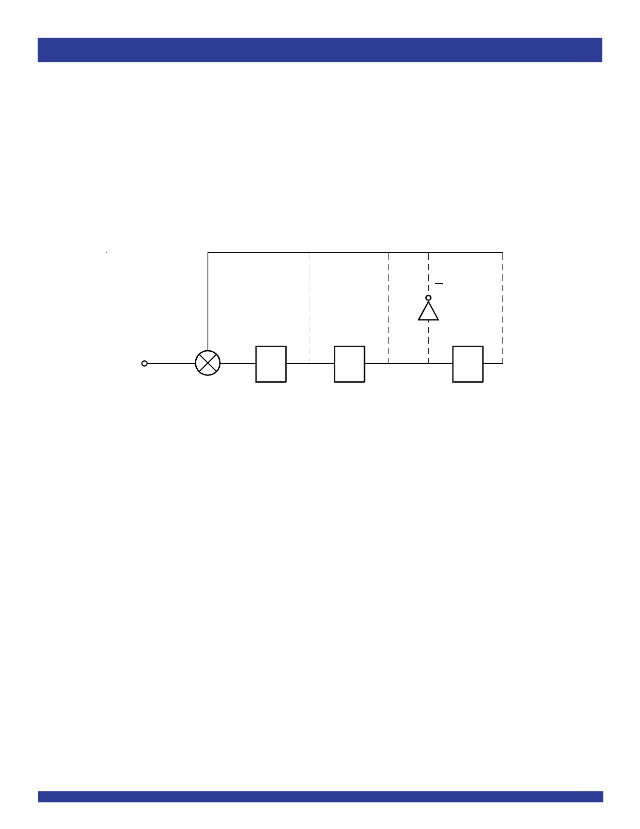
SIMPLIFIED DIAGRAM OF QS5LV919 FEEDBACK
2xQ
Q
Q
Q /2
IN P U T
VCO
/2
/2
PHASE
DETECTOR
The phase difference between the output and the input frequencies feeds
the VCO which drives the outputs. Whichever output is fed back, it will
stabilize at the same frequency as the input. Hence, this is a true negative
feedback closed loop system. In most applications, the output will optimally
have zero phase shift with respect to the input. In fact, the internal loop filter
on the QS5LV919 typically provides within 150ps of phase shift between
input and output.
If the user wishes to vary the phase difference (typically to compensate
for backplane delays), this is most easily accomplished by adding delay
circuits to the feedback path. The respective output used for feedback will
be advanced by the amount of delay in the feedback path. All other outputs
will retain their proper relationships to that output.
7
Share Link: 