DSP56001FE33 View Datasheet(PDF) - Motorola => Freescale
Part Name
Description
Manufacturer
DSP56001FE33 Datasheet PDF : 64 Pages
| |||
DSP56001 Electrical Characteristics
Electrical Specifications
The DSP is fabricated in high density CMOS with TTL compatible inputs and outputs.
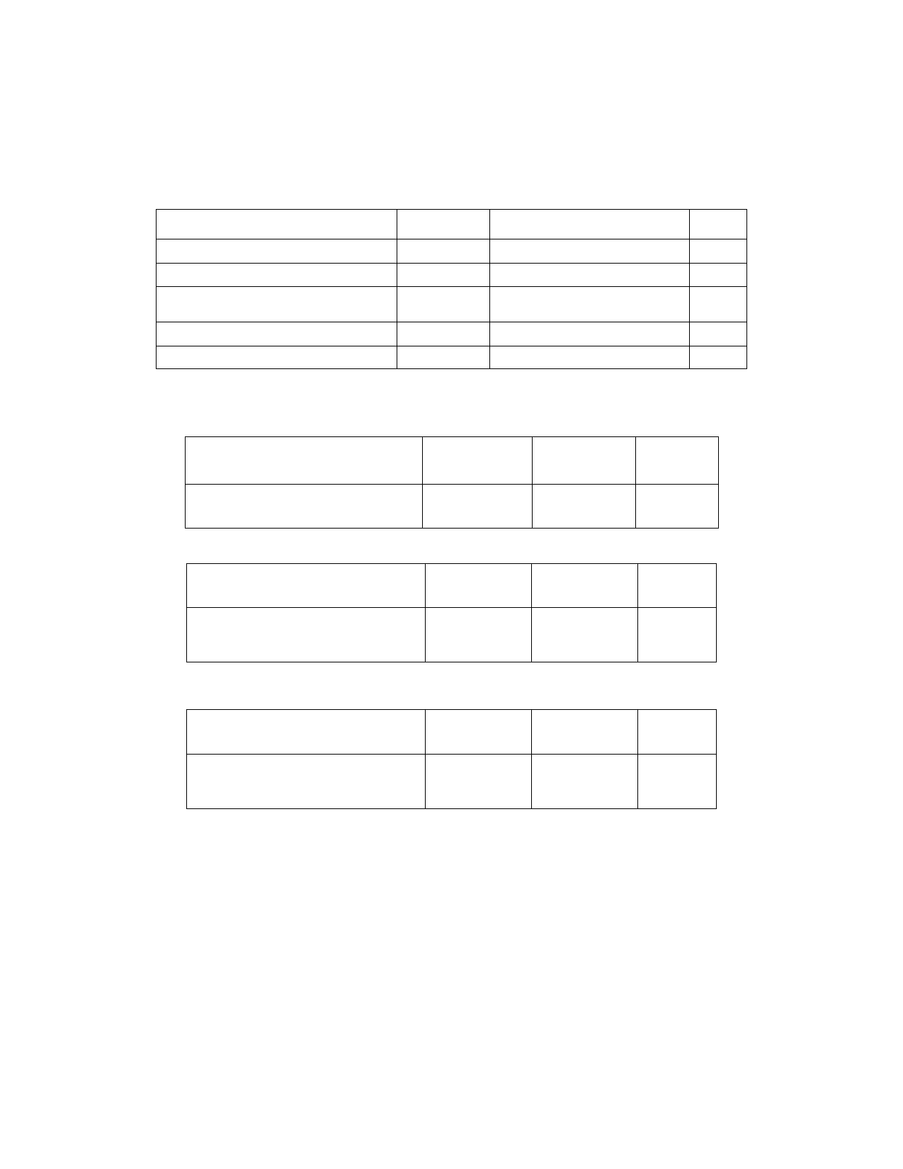
Maximum Ratings (VSS = 0 Vdc)
Rating
Supply Voltage
All Input Voltages
Current Drain per Pin
excluding Vcc and VSS
Operating Temperature Range
Storage Temperature
Symbol
Vcc
Vin
I
Value
-0.3 to +7.0
VSS- 0.5 to Vcc + 0.5
10
TJ
-40 to +105
Tstg
-55 to +150
Maximum Electrical Ratings
Unit
V
V
mA
°C
°C
Thermal Characteristics - PGA Package
Characteristics
Thermal Resistance - Ceramic
Junction to Ambient
Junction to Case (estimated)
Thermal Characteristics - CQFP Package
Characteristics
Thermal Resistance - Ceramic
Junction to Ambient
Junction to Case (estimated)
Symbol
ΘJA
ΘJC
Symbol
ΘJA
ΘJC
Value
27
6.5
Rating
°C/W
°C/W
Value
40
7.0
Rating
°C/W
°C/W
Thermal Characteristics - PQFP Package
Characteristics
Thermal Resistance - Plastic
Junction to Ambient
Junction to Case (estimated)
Symbol
ΘJA
ΘJC
Value
38
13.0
Rating
°C/W
°C/W
This device contains circuitry protecting against damage due to high static voltage or electrical fields; however, it is advised that normal
precautions be taken to avoid application of any voltages higher than maximum-rated voltages to this high-impedance circuit. Reliability
of operation is enhanced if unused inputs are tied to an appropriate logic voltage level (e.g., either Gnd or Vcc).
DSP56001
MOTOROLA
5
Share Link: 