ICS8343 View Datasheet(PDF) - Integrated Circuit Systems
Part Name
Description
Manufacturer
ICS8343 Datasheet PDF : 7 Pages
| |||
Integrated
Circuit
Systems, Inc.
ICS8343
LOW SKEW 1-TO-16
FANOUT BUFFER
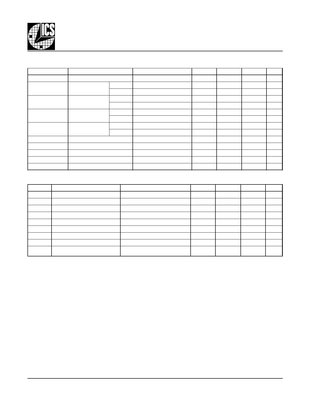
TABLE 4C. DC ELECTRICAL CHARACTERISTICS, VDD = VDD1 = VDD2 = 2.5V±5%, TA = 0° TO 70°C
Symbol
Parameter
Test Conditions
Minimum Typical
VDD, VDD1, VDD2 Operating Supply Voltage
2.375
2.5
VIH
Input High Voltage CLK
VDD = 2.625
2
OEx
VDD = 2.625
2
VIL
Input Low Voltage CLK
VDD = 2.375
-0.3
OEx
VDD = 2.375
-0.3
IIH
Input High Current CLK
VIN = VDD
OEx
VIN = VDD
IIL
Input Low Current CLK
VIN = 0V
-10
OEx
VIN = 0V
-10
IDD
Input Operating Supply Current
VOH
Output High Voltage
VDD = 2.375V, IOH = -25mA
1.5
VOL
Output Low Voltage
VDD = 2.375V, IOL = 25mA
IOZH
High Impedance Leakage Current
OEx = 0V, VOUT = VDD
IOZL
High Impedance Leakage Current
OEx = 0V, VOUT = 0V
-1
Maximum
2.625
VDD + 0.3
VDD + 0.3
0.7
0.8
1
1
100
0.8
1
Units
V
V
V
V
V
µA
µA
µA
µA
µA
V
V
µA
µA
TABLE 5C. AC ELECTRICAL CHARACTERISTICS, VDD = VDD1 = VDD2 = 2.5V±5%, TA = 0° TO 70°C
Symbol Parameter
Test Conditions
Minimum Typical Maximum Units
fMAX
Maximum Input Frequency
133
MHz
tpLH
Propagation Delay, Low-to-High
0 < f ≤ 200MHz
1.0
2.5
3.7
ns
tpHL
Propagation Delay, High-to-Low
0< f ≤ 200MHz
1.4
2.6
3.5
ns
tsk(o)
Output Skew; NOTE 3
Measured on rising edge @VDDx/2
250
ps
tsk(p)
Process Skew; NOTE 4
Measured on rising edge @VDDx/2
500
ps
tsk(pp)
Part-to-Part Skew; NOTE 5
Measured on rising edge @VDDx/2
750
ps
tR
Output Rise Time
0.5
0.8
ns
tF
Output Fall Time
0.9
1.7
ns
tPW
Output Pulse Width
tCYCLE/2
- 0.75
tCYCLE/2
tCYCLE/2
+ 0.75
ns
NOTE 1: All parameters measured at fMAX unless noted otherwise.
NOTE 2: Outputs terminated with 50Ω resistor connected to VDDx/2.
NOTE 3: Defined as skew across outputs at the same supply voltages and with equal load conditions.
NOTE 4: Defined as skew at the same output on different devices operating at the same supply voltages and with equal load conditions.
NOTE 5: Defined as skew at different outputs on different devices operating at the same supply voltages and with equal load conditions.
8343
www.icst.com
5
REV. C, 07072000
Share Link: 