MMDF2N02ER2 View Datasheet(PDF) - Motorola => Freescale
Part Name
Description
Manufacturer
MMDF2N02ER2 Datasheet PDF : 10 Pages
| |||
MMDF2N02E
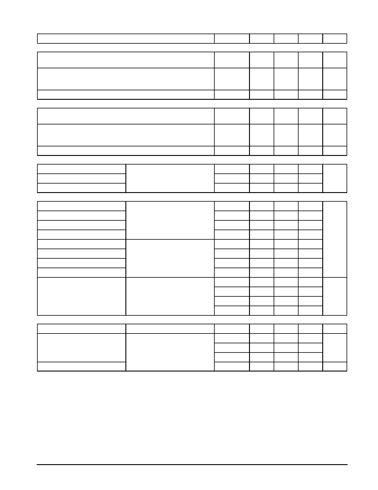
ELECTRICAL CHARACTERISTICS (TA = 25°C unless otherwise noted)
Characteristic
Symbol
Min
Typ
Max
Unit
OFF CHARACTERISTICS
Drain–to–Source Breakdown Voltage
(VGS = 0 Vdc, ID = 250 µAdc)
V(BR)DSS
Vdc
25
—
—
Zero Gate Voltage Drain Current
(VDS = 20 Vdc, VGS = 0 Vdc)
(VDS = 20 Vdc, VGS = 0 Vdc, TJ = 125°C)
IDSS
µAdc
—
—
1.0
—
—
10
Gate–Body Leakage Current (VGS = ± 20 Vdc, VDS = 0)
ON CHARACTERISTICS(1)
IGSS
—
—
100
nAdc
Gate Threshold Voltage
(VDS = VGS, ID = 250 µAdc
VGS(th)
Vdc
1.0
2.0
3.0
Static Drain–to–Source On–Resistance
(VGS = 10 Vdc, ID = 2.2 Adc)
(VGS = 4.5 Vdc, ID = 1.0 Adc)
RDS(on)
Ohm
—
0.083 0.100
—
0.110 0.200
Forward Transconductance (VDS = 3.0 Vdc, ID = 1.0 Adc)
gFS
1.0
2.6
—
Mhos
DYNAMIC CHARACTERISTICS
Input Capacitance
Output Capacitance
Transfer Capacitance
SWITCHING CHARACTERISTICS(2)
(VDS = 16 Vdc, VGS = 0 Vdc,
f = 1.0 MHz)
Ciss
Coss
Crss
—
380
532
pF
—
235
329
—
55
110
Turn–On Delay Time
Rise Time
Turn–Off Delay Time
Fall Time
(VDD = 10 Vdc, ID = 2.0 Adc,
VGS = 10 Vdc,
RG = 6.0 Ω)
td(on)
tr
td(off)
tf
—
7.0
21
ns
—
17
30
—
27
48
—
18
30
Turn–On Delay Time
Rise Time
Turn–Off Delay Time
Fall Time
(VDD = 10 Vdc, ID = 2.0 Adc,
VGS = 4.5 Vdc,
RG = 9.1 Ω)
td(on)
tr
td(off)
tf
—
10
30
—
35
70
—
19
38
—
25
50
Gate Charge
QT
—
10.6
30
nC
(VDS = 16 Vdc, ID = 2.0 Adc,
VGS = 10 Vdc)
Q1
—
1.3
—
Q2
—
2.9
—
Q3
—
2.7
—
SOURCE–DRAIN DIODE CHARACTERISTICS
Forward On–Voltage(1)
(IS = 2.0 Adc, VGS = 0 Vdc)
VSD
—
1.0
1.4
Vdc
Reverse Recovery Time
See Figure 11
(IS = 2.0 Adc, VGS = 0 Vdc,
dIS/dt = 100 A/µs)
trr
—
34
66
ns
ta
—
17
—
tb
—
17
—
Reverse Recovery Storage Charge
(1) Pulse Test: Pulse Width ≤ 300 µs, Duty Cycle ≤ 2%.
(2) Switching characteristics are independent of operating junction temperature.
QRR
—
0.03
—
µC
2
Motorola TMOS Power MOSFET Transistor Device Data
Share Link: 