MT48LC16M16A2BB-6A(2007) View Datasheet(PDF) - Micron Technology
Part Name
Description
Manufacturer
MT48LC16M16A2BB-6A Datasheet PDF : 77 Pages
| |||
256Mb: x4, x8, x16 SDRAM
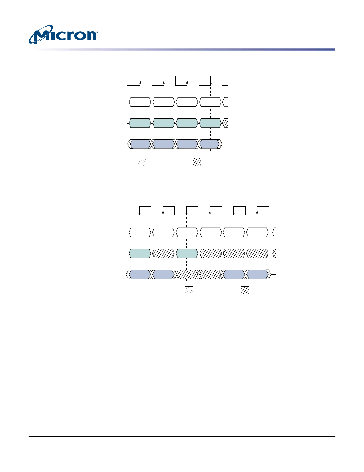
Timing Diagrams
Figure 41: Read – Without Auto Precharge
T0
CLK
T1
tCK
tCKS tCKH
CKE
tCMS tCMH
COMMAND
ACTIVE
NOP
T2
tCL
tCH
READ
T3
NOP
DQM/
DQML, DQMU
A0–A9,
A11, A12
A10
BA0, BA1
tAS tAH
ROW
tAS tAH
ROW
tAS tAH
BANK
tCMS tCMH
COLUMN m 2
DISABLE AUTO PRECHARGE
BANK
DQ
tRCD
tRAS
tRC
tAC
tLZ
CAS Latency
T4
NOP
tAC
tOH
DOUT m
T5
T6
T7
NOP
PRECHARGE
NOP
tAC
tOH
DOUT m + 1
ALL BANKS
SINGLE BANK
BANK
tAC
tOH
DOUT m + 2
tRP
tOH
DOUT m + 3
tHZ
T8
ACTIVE
ROW
ROW
BANK
DON’T CARE
UNDEFINED
Notes:
1. For this example, BL = 4, CL = 2, and the READ burst is followed by a “manual” PRECHARGE.
2. x16: A9, A11, and A12 = “Don’t Care”
x8: A11 and A12 = “Don’t Care”
x4: A12 = “Don’t Care”
PDF: 09005aef8091e6d1/Source: 09005aef8091e6a8
256MSDRAM_2.fm - Rev. L 10/07 EN
61
Micron Technology, Inc., reserves the right to change products or specifications without notice.
©1999 Micron Technology, Inc. All rights reserved.
Share Link: 