AD8313 View Datasheet(PDF) - Analog Devices
Part Name
Description
Manufacturer
AD8313 Datasheet PDF : 24 Pages
| |||
AD8313
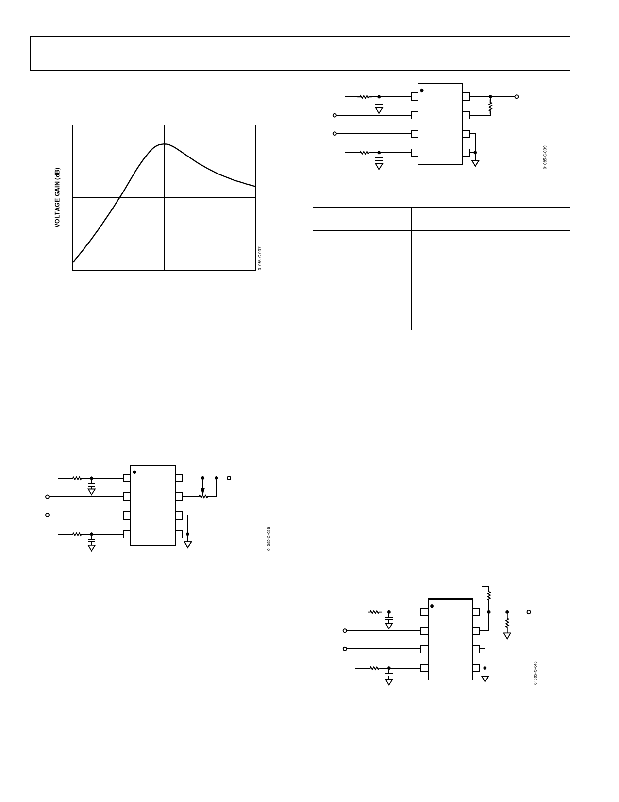
Figure 37 shows the voltage response of the 100 MHz matching
network. Note the high attenuation at lower frequencies typical
of a high-pass network.
15
10
5
0
–5
50
100
200
FREQUENCY (MHz)
Figure 37. Voltage Response of 100 MHz Narrow-Band Matching Network
ADJUSTING THE LOG SLOPE
Figure 38 shows how the log slope can be adjusted to an exact
value. The idea is simple: the output at the VOUT pin is attenu-
ated by the variable resistor R2 working against the internal 18 kΩ
of input resistance at the VSET pin. When R2 is 0, the attenu-
ation it introduces is 0, and thus the slope is the basic 18 mV/dB.
Note that this value varies with frequency, (Figure 10). When
R2 is set to its maximum value of 10 kΩ, the attenuation from
VOUT to VSET is the ratio 18/(18 + 10), and the slope is raised
to (28/18) × 18 mV, or 28 mV/dB. At about the midpoint, the
nominal scale is 23 mV/dB. Thus, a 70 dB input range changes
the output by 70 × 23 mV, or 1.6 V.
R1
10
+VS
1 VPOS VOUT 8
0.1F
AD8313
2 INHI VSET 7
3 INLO COMM 6
R3
10
+VS
4 VPOS PWDN 5
0.1F
R2
10k
18–30mV/dB
Figure 38. Adjusting the Log Slope
As stated, the unadjusted log slope varies with frequency from
17 mV/dB to 20 mV/dB, as shown in Figure 10. By placing a
resistor between VOUT and VSET, the slope can be adjusted to
a convenient 20 mV/dB as shown in Figure 39.
Table 6 shows the recommended values for this resistor, REXT.
Also shown are values for REXT, which increase the slope to
approximately 50 mV/dB. The corresponding voltage swings
for a −65 dBm to 0 dBm input range are also shown in Table 7.
Data Sheet
R1
10
+VS
1 VPOS VOUT 8
0.1F
AD8313
2 INHI VSET 7
REXT
20mV/dB
3 INLO COMM 6
R3
10
+VS
4 VPOS PWDN 5
0.1F
Figure 39. Adjusting the Log Slope to a Fixed Value
Table 6. Values for REXT in Figure 39
Frequency REXT
MHz
kV
Slope VOUT Swing for Pin
mV/dB −65 dBm to 0 dBm – V
100
0.953 20
0.44 to 1.74
900
2.00 20
0.58 to 1.88
1900
2.55 20
0.70 to 2.00
2500
0
20
0.54 to 1.84
100
29.4 50
1.10 to 4.35
900
32.4 50.4
1.46 to 4.74
1900
33.2 49.8
1.74 to 4.98
2500
26.7 49.7
1.34 to 4.57
The value for REXT is calculated by
REXT
New
Slope Original
Original Slope
Slope 18 k
The value for the Original Slope, at a particular frequency, can
be read from Figure 10. The resulting output swing is calculated
by simply inserting the New Slope value and the intercept at that
frequency (Figure 10 and Figure 13) into the general equation
for the AD8313’s output voltage:
VOUT = Slope(PIN − Intercept)
INCREASING OUTPUT CURRENT
To drive a more substantial load, either a pull-up resistor or an
emitter-follower can be used.
In Figure 40, a 1 kΩ pull-up resistor is added at the output,
which provides the load current necessary to drive a 1 kΩ load
to 1.7 V for VS = 2.7 V. The pull-up resistor slightly lowers the
intercept and the slope. As a result, the transfer function of the
AD8313 is shifted upward (intercept shifts downward).
+VS
R1
1k
10
+VS
1 VPOS VOUT 8
0.1F
AD8313
2 INHI VSET 7
20mV/dB
RL = 1k
3 INLO COMM 6
R3
10
+VS
4 VPOS PWDN 5
0.1F
Figure 40. Increasing AD8313 Output Current Capability
Rev. E | Page 18 of 24
Share Link: 