SPC122A View Datasheet(PDF) - Unspecified
Part Name
Description
Manufacturer
SPC122A Datasheet PDF : 20 Pages
| |||
Preliminary
SPC122A
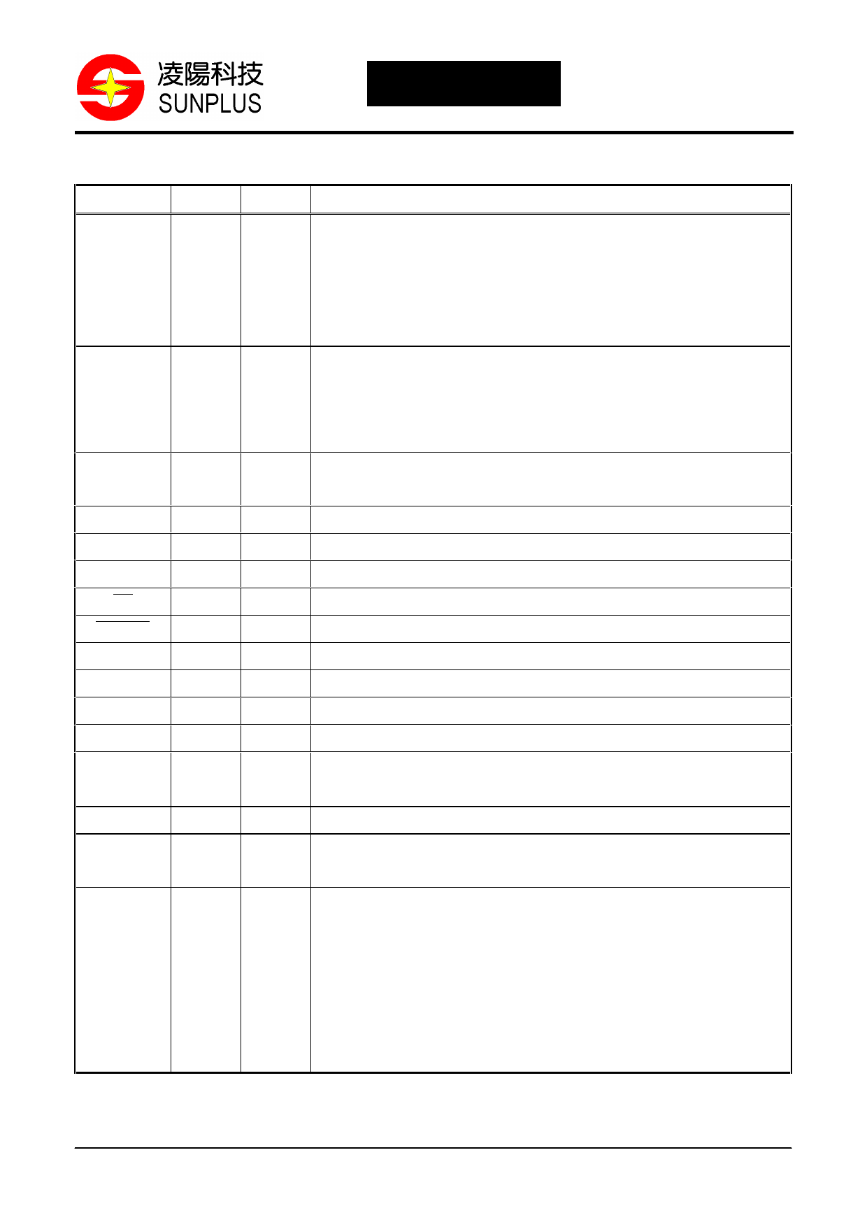
PIN DESCRIPTIONS*
Mnemonic PIN No.
VDD
5
29
34
45
57
VSS
17
27
50
66
XI
32
XO
OPT*
BURN
CE
ROMOE
SPOP
A17
RESET
TEST
AUD1
AUD2
D7 – 0
A13 – 0
A16 – 14
31
30
15
16
14
18
4
19
36
33
35
6-13
74-60
3-1
IOA0
46
IOA1
47
IOA2
48
IOA3
49
Type
I
I
I
O
I
I
I
I/O
I
O
I
I
O
O
I/O
I/O
I/O
I/O
I/O
I/O
Description
Positive supply for logic and I/O pins
Ground reference for logic and I/O pins
Oscillator crystal input or RESISTOR (Resistor should be connected to
VDD)
Oscillator crystal output
For ROSC option, OPT should be connected to VDD.
Burn, This pin is an active high to select the flash ROM program function
This pin is an active low to select this chip as a 1Mbits memory
Data Output enable
Serial program option
Extended Memory Enable
This pin is an active low reset to the chip.
TEST MODE
AUDIO OUTPUT
Data Bus
Address Bus
Port A is an 8-bit bi-directional programmable Input / Output port with
Pull-high or Open-drain option. As inputs, Port A can be in either the
Pure or Pull-high states. As outputs, Port A can be either Buffer or
Open-drain NMOS types (Sink current).
IOA0: Serial programming clock output
IOA2: Multi-duty cycle output
**See note 1 and 2 below.
Sunplus Technology Co., Ltd.
8
Rev.: 0.3 1999.11.18
Share Link: 