5962-9313301MPA View Datasheet(PDF) - Analog Devices
Part Name
Description
Manufacturer
5962-9313301MPA Datasheet PDF : 16 Pages
| |||
20pF
1kΩ
+VS
**
1kΩ
VIN
2
7
AD797 6
3
4
**
VOUT
–VS
** SEE FIGURE 32
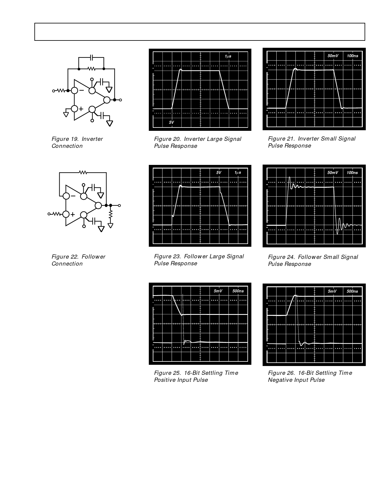
Figure 19. Inverter
Connection
1µs
100
90
10
0%
5V
Figure 20. Inverter Large Signal
Pulse Response
AD797
50mV 100ns
100
90
10
0%
Figure 21. Inverter Small Signal
Pulse Response
100Ω
+VS
**
2
7
RS* AD797 6
VIN
3
4
**
VOUT
600Ω
–VS
* VALUE OF SOURCE RESISTANCE –
SEE TEXT
** SEE FIGURE 32
Figure 22. Follower
Connection
5V
1µs
50mV 100ns
100
100
90
90
10
10
0%
0%
Figure 23. Follower Large Signal
Pulse Response
Figure 24. Follower Small Signal
Pulse Response
See Figure 40 for settling time
test circuit.
5mV 500ns
5mV
500ns
100
100
90
90
10
0%
Figure 25. 16-Bit Settling Time
Positive Input Pulse
10
0%
Figure 26. 16-Bit Settling Time
Negative Input Pulse
REV. C
–7–
Share Link: 