ADA4853-1 View Datasheet(PDF) - Analog Devices
Part Name
Description
Manufacturer
ADA4853-1 Datasheet PDF : 16 Pages
| |||
ABSOLUTE MAXIMUM RATINGS
Table 3.
Parameter
Supply Voltage
Power Dissipation
Common-Mode Input Voltage
Differential Input Voltage
Storage Temperature Range
Operating Temperature Range
6-Lead SC70
16-Lead LFCSP_VQ
14-Lead TSSOP
Lead Temperature
Junction Temperature
Rating
5.5 V
See Figure 6
−VS − 0.2 V to +VS − 1.2 V
±VS
−65°C to +125°C
−40°C to +85°C
−40°C to +105°C
−40°C to +105°C
JEDEC J-STD-20
150°C
Stresses above those listed under Absolute Maximum Ratings
may cause permanent damage to the device. This is a stress
rating only; functional operation of the device at these or any
other conditions above those indicated in the operational
section of this specification is not implied. Exposure to absolute
maximum rating conditions for extended periods may affect
device reliability.
THERMAL RESISTANCE
θJA is specified for the worst-case conditions, that is, θJA is
specified for the device soldered in the circuit board for surface-
mount packages.
Table 4.
Package Type
6-Lead SC70
16-Lead LFCSP_VQ
14-Lead TSSOP
θJA
Unit
430
°C/W
63
°C/W
120
°C/W
Maximum Power Dissipation
The maximum safe power dissipation for the ADA4853-1/
ADA4853-2/ADA4853-3 is limited by the associated rise in
junction temperature (TJ) on the die. At approximately 150°C,
which is the glass transition temperature, the plastic changes its
properties. Even temporarily exceeding this temperature limit
can change the stresses that the package exerts on the die,
permanently shifting the parametric performance of the
amplifiers. Exceeding a junction temperature of 150°C for an
extended period can result in changes in silicon devices,
potentially causing degradation or loss of functionality.
ADA4853-1/ADA4853-2/ADA4853-3
The power dissipated in the package (PD) for a sine wave and a
resistor load is the total power consumed from the supply
minus the load power.
PD = Total Power Consumed − Load Power
( ) PD = VSUPPLY VOLTAGE × ISUPPLY CURRENT
– VOUT 2
RL
RMS output voltages should be considered.
Airflow increases heat dissipation, effectively reducing θJA.
In addition, more metal directly in contact with the package
leads and through holes under the device reduces θJA.
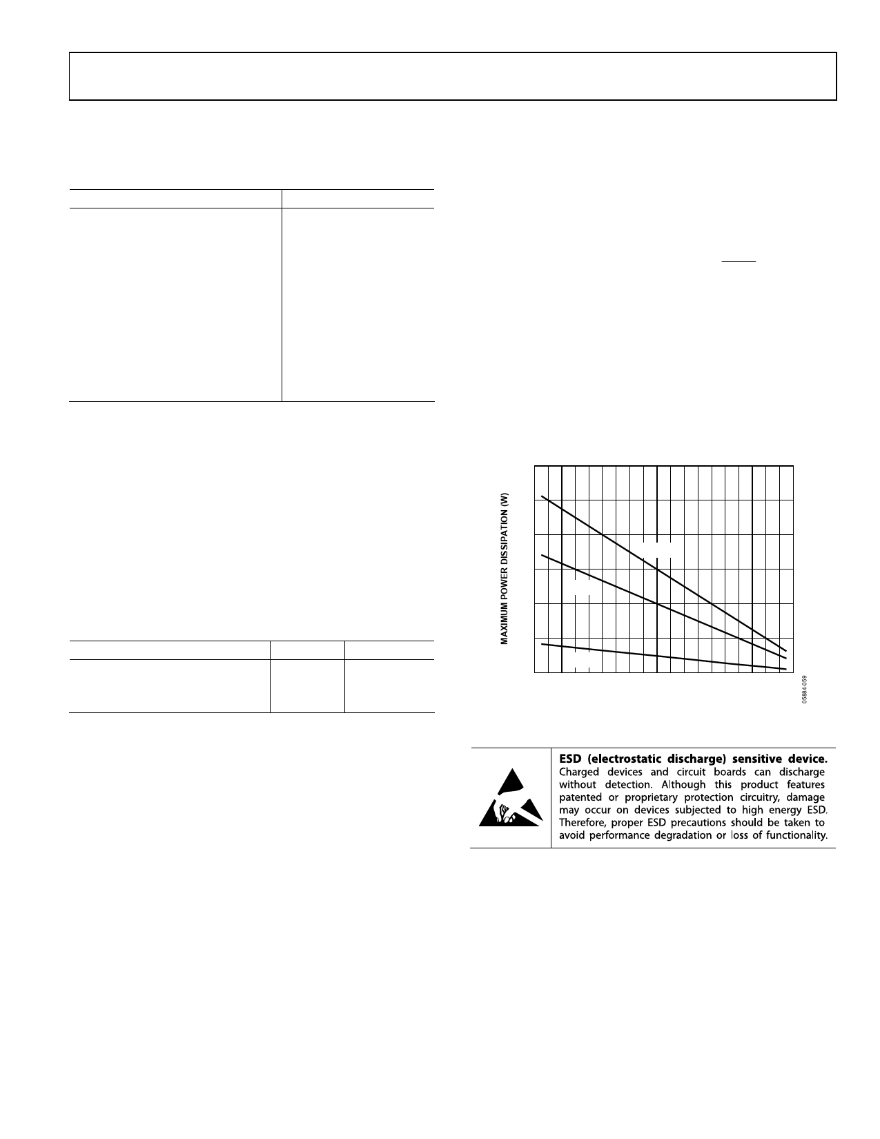
Figure 6 shows the maximum safe power dissipation in the
package vs. the ambient temperature for the 6-lead SC70
(430°C/W), the 14-lead TSSOP (120°C/W), and the 16-lead
LFCSP_VQ (63°C/W) on a JEDEC standard 4-layer board. θJA
values are approximations.
3.0
2.5
2.0
1.5
TSSOP
1.0
LFCSP
0.5
SC70
0
–55 –35 –15 5
25 45 65 85 105 125
AMBIENT TEMPERATURE (°C)
Figure 6. Maximum Power Dissipation vs. Temperature for a 4-Layer Board
ESD CAUTION
Rev. B | Page 5 of 16
Share Link: 