ADG633YCPZ(RevB) View Datasheet(PDF) - Analog Devices
Part Name
Description
Manufacturer
ADG633YCPZ Datasheet PDF : 16 Pages
| |||
Data Sheet
PIN CONFIGURATIONS AND FUNCTION DESCRIPTIONS
ADG633
S2B 1
S2A 2
S3B 3
D3 4
S3A 5
EN 6
VSS 7
GND 8
16 VDD
15 D2
ADG633
TOP VIEW
(Not to Scale)
14 D1
13 S1B
12 S1A
11 A0
10 A1
9 A2
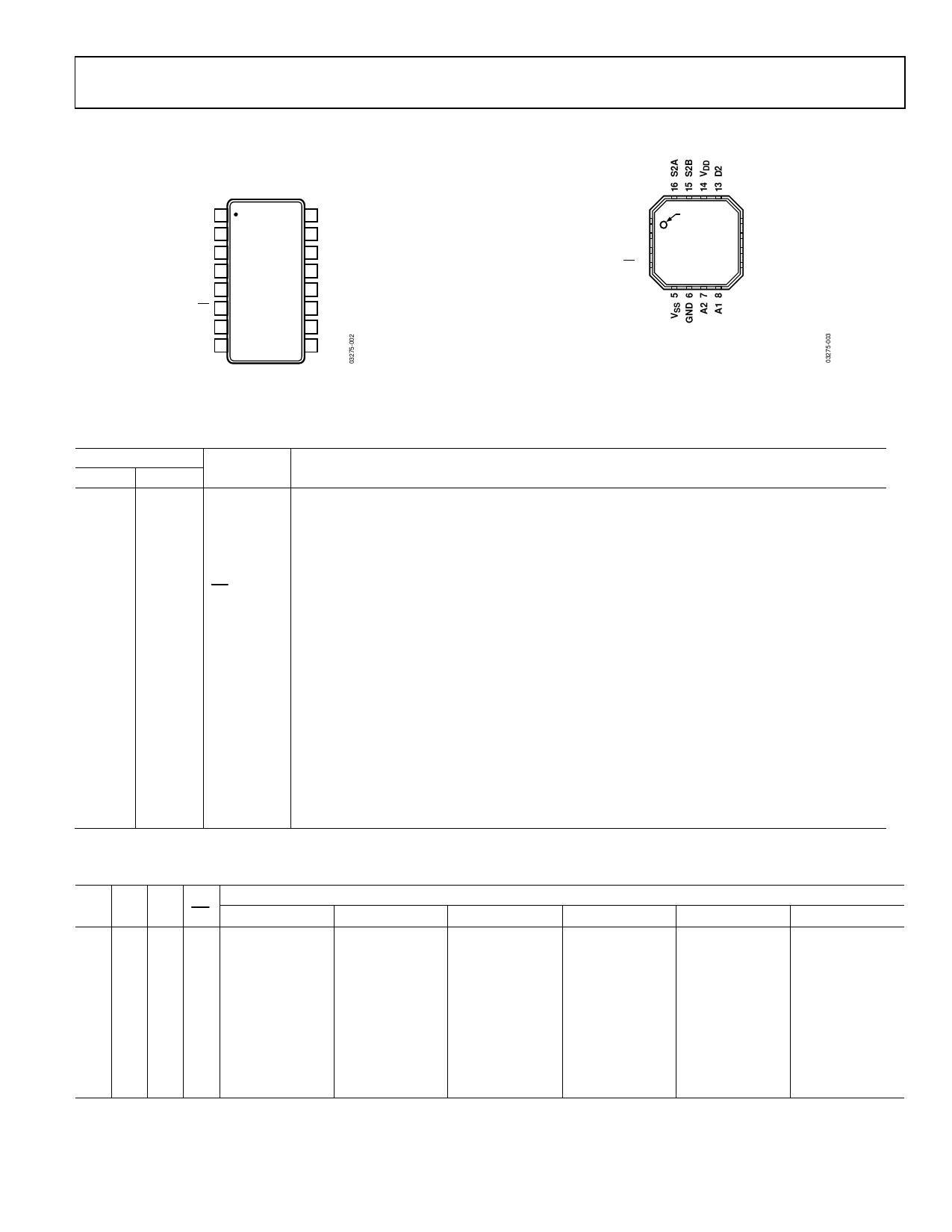
Figure 2. 16-Lead TSSOP Pin Configuration
S3B 1
D3 2
S3A 3
EN 4
ADG633
TOP VIEW
(Not to Scale)
12 D1
11 S1B
10 S1A
9 A0
NOTES
1. THE EXPOSED PADDLE CAN BE LEFT FLOATING
OR BE TIED TO VDD, VSS, OR GND.
Figure 3. 16-Lead LFCSP Pin Configuration
Table 5. Pin Function Descriptions
Pin No.
TSSOP
LFCSP Mnemonic
1
15
S2B
2
16
S2A
3
1
S3B
4
2
D3
5
3
S3A
6
4
EN
7
5
VSS
8
6
GND
9
7
A2
10
8
A1
11
9
A0
12
10
S1A
13
11
S1B
14
12
D1
15
13
D2
16
14
VDD
Not applicable EP
EP
Description
Source Terminal of Multiplexer 2. Can be an input or output.
Source Terminal of Multiplexer 2. Can be an input or output.
Source Terminal of Multiplexer 3. Can be an input or output.
Drain Terminal of Multiplexer 3. Can be an input or output.
Source Terminal of Multiplexer 3. Can be an input or output.
Digital Control Input. Disables all multiplexers when set high.
Most Negative Power Supply Terminal. Tie this pin to GND when using the device with single-supply
voltages.
Ground (0 V) Reference.
Digital Control Input.
Digital Control Input.
Digital Control Input.
Source Terminal of Multiplexer 1. Can be an input or output.
Source Terminal of Multiplexer 1. Can be an input or output.
Drain Terminal of Multiplexer 1. Can be an input or output.
Drain Terminal of Multiplexer 2. Can be an input or output.
Most Positive Power Supply Terminal.
Exposed Paddle. The exposed paddle can be left floating or be tied to VDD, VSS, or GND.
Table 6. ADG633 Truth Table
A2 A1 A0 EN Switch S1A/D1
X1 X1 X1 1 Off
0 0 0 0 On
0 0 1 0 Off
0 1 0 0 On
0 1 1 0 Off
1 0 0 0 On
1 0 1 0 Off
1 1 0 0 On
1 1 1 0 Off
Switch S1B/D1
Off
Off
On
Off
On
Off
On
Off
On
1 X means the logic state does not matter; it can be either 0 or 1.
Switch Condition
Switch S2A/D2 Switch S2B/D2
Off
Off
On
Off
On
Off
Off
On
Off
On
On
Off
On
Off
Off
On
Off
On
Switch S3A/D3
Off
On
On
On
On
Off
Off
Off
Off
Switch S3B/D3
Off
Off
Off
Off
Off
On
On
On
On
Rev. B | Page 7 of 16
Share Link: 