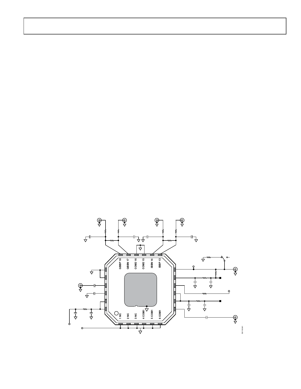
ADL5385(Rev0) View Datasheet(PDF) - Analog Devices
Part Name
Description
Manufacturer
ADL5385 Datasheet PDF : 24 Pages
| |||
APPLICATIONS
DAC MODULATOR INTERFACING
The ADL5385 is designed to interface with minimal components
to members of the Analog Devices family of digital-to-analog
converters (DAC). These DACs feature an output current swing
from 0 to 20 mA, and the interface described in this section can
be used with any DAC that has a similar output.
Driving the ADL5385 with an Analog Devices TxDAC®
An example of the interface using the AD9777 TxDAC is shown
in Figure 31. The baseband inputs of the ADL5385 require a dc
bias of 500 mV. The average output current on each of the
outputs of the AD9777 is 10 mA. Therefore, a single 50 Ω
resistor to ground from each of the DAC outputs results in an
average current of 10 mA flowing through each of the resistors,
thus producing the desired 500 mV dc bias for the inputs to the
ADL5385.
AD9777
73
IOUTA1
RBIP
50Ω
IOUTB1
RBIN
72 50Ω
ADL5385
13
IBBP
14
IBBN
IOUTB2
IOUTA2
69
RBQN
50Ω
RBQP
68 50Ω
17
QBBN
18
QBBP
Figure 31. Interface Between AD9777 and ADL5385 with 50 Ω Resistors to
Ground to Establish the 500 mV DC Bias for the ADL5385 Baseband Inputs
The AD9777 output currents have a swing that ranges from
0 to 20 mA. With the 50 Ω resistors in place, the ac voltage
swing going into the ADL5385 baseband inputs ranges from
0 V to 1 V. A full-scale sine wave out of the AD9777 can be
described as a 1 V p-p single-ended (or 2 V p-p differential)
sine wave with a 500 mV dc bias.
Limiting the AC Swing
There are situations in which it is desirable to reduce the
ac voltage swing for a given DAC output current. This can be
achieved through the addition of another resistor to the
interface. This resistor is placed in shunt between each side of
the differential pair, as illustrated in Figure 32. It has the effect
of reducing the ac swing without changing the dc bias already
established by the 50 Ω resistors.
ADL5385
AD9777
IOUTA1
IOUTB1
73
RBIP
50Ω
RBIN
72 50Ω
RSLI
100Ω
ADL5385
13
IBBP
14
IBBN
IOUTB2
IOUTA2
69
RBQN
50Ω
RBQP
68 50Ω
RSLQ
100Ω
17
QBBN
18
QBBP
Figure 32. AC Voltage Swing Reduction Through Introduction of Shunt
Resistor Between Differential Pair
The value of this ac voltage swing-limiting resistor is chosen
based on the desired ac voltage swing. Figure 33 shows the
relationship between the swing-limiting resistor and the peak-
to-peak ac swing that it produces when 50 Ω bias-setting
resistors are used.
2.0
1.8
1.6
1.4
1.2
1.0
0.8
0.6
0.4
0.2
0
10
100
1000
10000
RL (Ω)
Figure 33. Relationship Between AC Swing-Limiting Resistor and
Peak-to-Peak Voltage Swing with 50 Ω Bias-Setting Resistors
Filtering
When driving a modulator from a DAC, it is necessary to
introduce a low-pass filter between the DAC and the modulator
to reduce the DAC images. The interface for setting up the
biasing and ac swing lends itself well to the introduction of such
a filter. The filter can be inserted in between the dc bias setting
resistors and the ac swing-limiting resistor, thus establishing the
input and output impedances for the filter.
Examples of filters are discussed in the 155 MBPS (STM-1) 128
QAM Transmitter and the CMTS Transmitter Application
sections.
Rev. 0 | Page 15 of 24
Share Link: 