ADP1707ARDZ-0.8-R7 View Datasheet(PDF) - Analog Devices
Part Name
Description
Manufacturer
ADP1707ARDZ-0.8-R7 Datasheet PDF : 20 Pages
| |||
PCB LAYOUT CONSIDERATIONS
Heat dissipation from the package can be improved by
increasing the amount of copper attached to the pins of the
ADP1706/ADP1707/ADP1708. However, as can be seen from
Table 5, a point of diminishing returns is eventually reached,
beyond which an increase in the copper size does not yield
significant heat dissipation benefits.
The ADP1706/ADP1707/ADP1708 feature an exposed pad on
the bottom of both the SOIC and LFCSP packages to improve
thermal performance. Because the exposed pad is electrically
connected to GND inside the package, it is recommended that
it also be connected to the ground plane on the PCB with a
sufficient amount of copper.
Here are a few general tips when designing PCBs:
• Place the input capacitor as close as possible to the IN and
GND pins.
• Place the output capacitor as close as possible to the OUT
and GND pins.
• For the ADP1706, place the soft start capacitor as close as
possible to the SS pin.
• Connect the load as close as possible to the OUT and
SENSE pins.
ADP1706/ADP1707/ADP1708
Use of 0402 or 0603 size capacitors and resistors achieves the
smallest possible footprint solution on boards where area is
limited.
ANALOG
DEVICES
ADP1706/ADP1707/ADP1708
SOIC8
GND
C1
C3
C2
GND
U1
R1
J1
R2
VIN
VOUT
GND
EN
ADJ/TRK/SS
GND
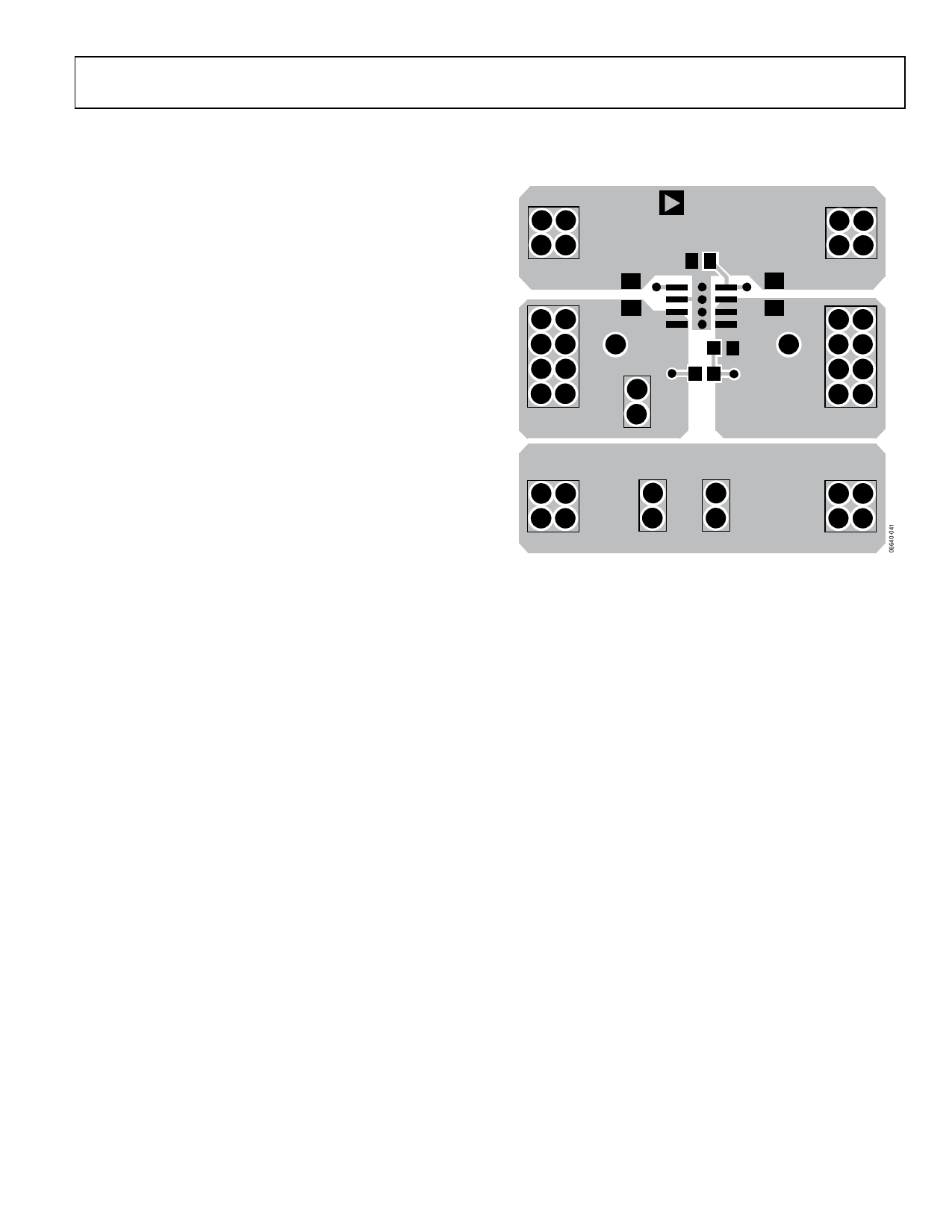
Figure 42. Example PCB Layout
Rev. 0 | Page 15 of 20
Share Link: 