ADUM2211 View Datasheet(PDF) - Analog Devices
Part Name
Description
Manufacturer
ADUM2211 Datasheet PDF : 17 Pages
| |||
Data Sheet
ADuM2210/ADuM2211
ELECTRICAL CHARACTERISTICS—MIXED 5 V/3.3 V OPERATION
All voltages are relative to their respective ground. 4.5 V ≤ VDD1 ≤ 5.5 V, 3.0 V ≤ VDD2 ≤ 3.6 V. All minimum/maximum specifications
apply over the entire recommended operation range, −40°C ≤ TA ≤ 125°C, unless otherwise noted. All typical specifications are at TA =
25°C, VDD1 = 5 V, VDD2 = 3.3 V.
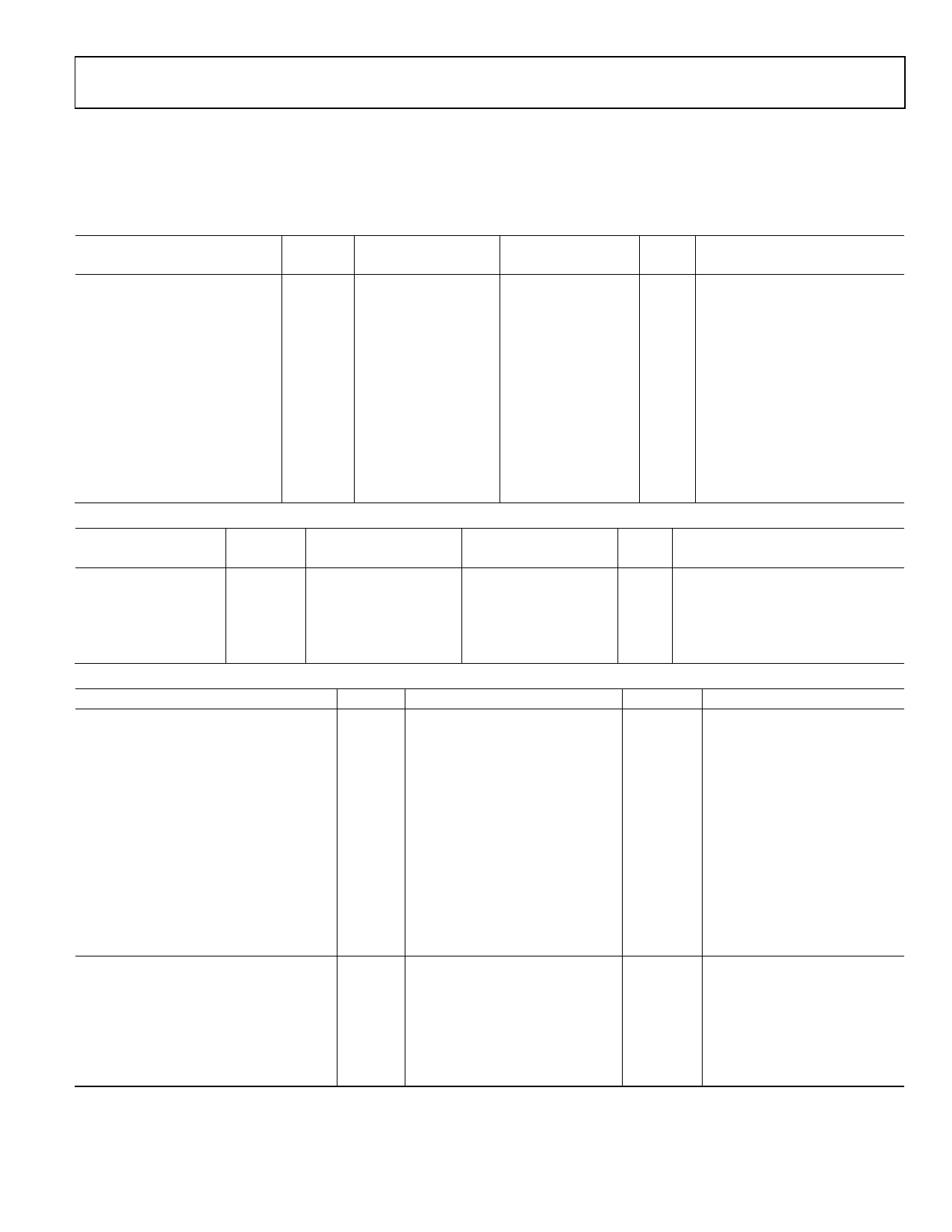
Table 7.
Parameter
SWITCHING SPECIFICATIONS
Pulse Width
Data Rate
Propagation Delay
Pulse Width Distortion
S Grade and T Grade
W Grade
Change vs. Temperature
Propagation Delay Skew
Channel Matching
Codirectional
Opposing-Direction
S Grade
T Grade
Symbol Min Typ Max Min Typ Max Unit
Test Conditions/Comments
PW
1000
tPHL, tPLH
15
PWD
tPSK
100
ns
Within PWD limit
1
10 Mbps Within PWD limit
150 15
55 ns
50% input to 50% output
40
3
ns
|tPLH − tPHL|
40
3
ns
40
4
ns
5
ps/°C
50
22 ns
Between any two units
tPSKCD
tPSKOD
50
3
ns
50
22 ns
Table 8.
Parameter
SUPPLY CURRENT
ADuM2210
ADuM2211
Symbol
IDD1
IDD2
IDD1
IDD2
1 Mbps, S Grade
10 Mbps, T Grade
Min Typ Max Min Typ Max Unit Test Conditions/Comments
No load
1.3 1.7
3.5 4.8
mA
0.7 1.0
1.1 1.9
mA
1.1 1.5
2.6 4.0
mA
0.8 1.6
1.9 2.5
mA
Table 9.
Parameter
DC SPECIFICATIONS
Logic High Input Threshold
Logic Low Input Threshold
Logic High Output Voltages
Logic Low Output Voltages
Input Current per Channel
Supply Current per Channel
Quiescent Input Supply Current
Quiescent Output Supply Current
Dynamic Input Supply Current
Dynamic Output Supply Current
AC SPECIFICATIONS
Output Rise/Fall Time
ADuM2210/ADuM2211 S Grade
ADuM2210/ADuM2211 T Grade
Common-Mode Transient Immunity2
Refresh Period
Symbol Min
Typ
Max Unit
Test Conditions/Comments1
VIH
0.7VDDX
V
VIL
0.3VDDX V
VOH
VDDX − 0.1 VDDX
V
VDDX − 0.5 VDDX − 0.2
V
VOL
0.0
0.1
V
0.2
0.40
V
II
−10
+0.01
+10
µA
IOx = −20 µA, VIx = VIxH
IOx = −3.2 mA, VIx = VIxH
IOx = 20 µA, VIx = VIxL
IOx = 3.2 mA, VIx = VIxL
0 V ≤ VIX ≤ VDDX
IDDI (Q)
IDDO (Q)
IDDI (D)
IDDO (D)
0.4
0.8
mA
0.3
0.5
mA
0.19
mA/Mbps
0.03
mA/Mbps
tR/tF
10
3
|CM|
25
35
Tr
1.6
ns
ns
kV/µs
µs
10% to 90%
10% to 90%
VIx = VDDX, VCM = 1000 V,
transient magnitude = 800 V
1 IOx is the Channel x output current, where x = A or B, VIxH is the input side logic high, and VIxL is the input side logic low.
2 |CM| is the maximum common-mode voltage slew rate that can be sustained while maintaining VO > 0.8 VDDx. The common-mode voltage slew rates apply to both
rising and falling common-mode voltage edges.
Rev. F | Page 5 of 17
Share Link: 