MC141537T1 View Datasheet(PDF) - Motorola => Freescale
Part Name
Description
Manufacturer
MC141537T1 Datasheet PDF : 16 Pages
| |||
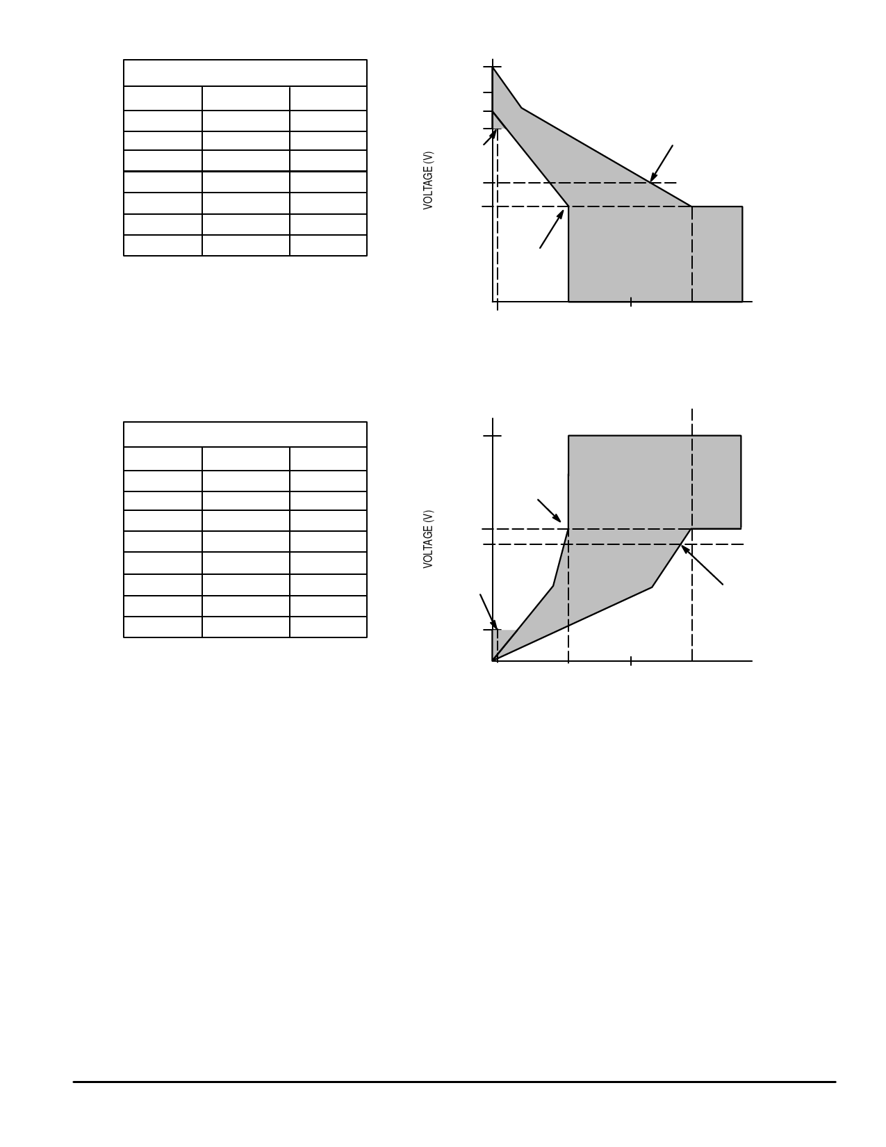
PULL–UP
3.6
VOLTAGE (V)
–0.5
0
1.4
1.65
2
3.135
3.6
I (mA) MIN
– 40
– 40
– 40
– 37
–28
0
0
I (mA) MAX
– 120
– 120
– 120
– 104
– 81
– 20
0
3.135
2.8
DC DRIVE
POINT
1.65
1.4
TEST POINT
AC DRIVE
POINT
0
0 –5
–40
– 80
–120
NOTES:
1. Driver impedance @ 1.65 V = 15.9 to 44.6 Ω.
CURRENT (mA)
2. Meets the temperature and voltage range specified in DC Characteristics tables.
3. This drawing is not to scale. Comparisons should be made to the table in Figure 2a.
a. Pull–Up
VOLTAGE (V)
–0.5
0
0.5
1
1.65
1.8
3.6
4
PULL–DOWN
I (mA) MIN
– 34
0
17
35
45
46
46
46
I (mA) MAX
– 126
0
47
90
114
120
120
120
VDD
AC DRIVE
POINT
1.8
1.65
DC DRIVE
POINT
0.3
0
05
46
80
NOTES:
CURRENT (mA)
1. Driver impedance @ 1.65 V = 15.9 to 44.6 Ω.
2. Meets the temperature and voltage range specified in DC Characteristics tables.
3. This drawing is not to scale. Comparisons should be made to the table in Figure 2b.
b. Pull–Down
Figure 2. Output Buffer Characteristics
TEST POINT
120
MCM64PE32•MCM64PE64
10
MOTOROLA FAST SRAM
Share Link: 