APU3073 View Datasheet(PDF) - Advanced Power Electronics Corp
Part Name
Description
Manufacturer
APU3073
Advanced Power Electronics Corp
APU3073 Datasheet PDF : 17 Pages
| |||
APU3073
LDO Section
Output Voltage Programming
Output voltage for LDO is programmed by reference volt-
age and external voltage divider. The Fb2 pin is the in-
verting input of the error amplifier, which is internally ref-
erenced to 0.8V. The divider is ratioed to provide 0.8V at
the Fb2 pin when the output is at its desired value. The
output voltage is defined by using the following equation
( ) VOUT2 = VREF3
1+
R7
R10
For:
VOUT2 = 1.6V
VREF = 0.8V
R10 = 1KV
Results to R7=1KV
APU3073
Fb2
VOUT2
R7
R10
Layout Consideration
The layout is very important when designing high fre-
quency switching converters. Layout will affect noise
pickup and can cause a good design to perform with
less than expected results.
Start to place the power components. Make all the con-
nections in the top layer with wide, copper filled areas.
The inductor, output capacitor and the MOSFET should
be close to each other as possible. This helps to reduce
the EMI radiated by the power traces due to the high
switching currents through them. Place input capacitor
directly to the drain of the high-side MOSFET. To reduce
the ESR, replace the single input capacitor with two par-
allel units. The feedback part of the system should be
kept away from the inductor and other noise sources
and be placed close to the IC. In multilayer PCB, use
one layer as power ground plane and have a separate
control circuit ground (analog ground), to which all sig-
nals are referenced. The goal is to localize the high cur-
rent path to a separate loop that does not interfere with
the more sensitive analog control function. These two
grounds must be connected together on the PC board
layout at a single point.
Figure 13 - Programming the output voltage for LDO.
LDO Power MOSFET Selection
The first step in selecting the power MOSFET for the
linear regulator is to select the maximum RDS(ON) based
on the input to the dropout voltage and the maximum
load current.
RDS(ON)
=
VIN(LDO) - VOUT2
IOUT2
For:
VIN(LDO) = 2.5V
VOUT2 = 1.6V
IOUT2 = 2A
Results to: RDS(ON)(MAX) = 0.45V
Note that since the MOSFET RDS(ON) increases with tem-
perature, this number must be divided by ~1.5 in order
to find the RDS(ON)(MAX) at room temperature. The IRLR2703
has a maximum of 0.065V RDS(ON) at room temperature,
which meets our requirements.
500
450
400
350
300
250
200
150
100
50
0
0
50 100 150 200 250 300 350 400 450 500 550
Rt (K V)
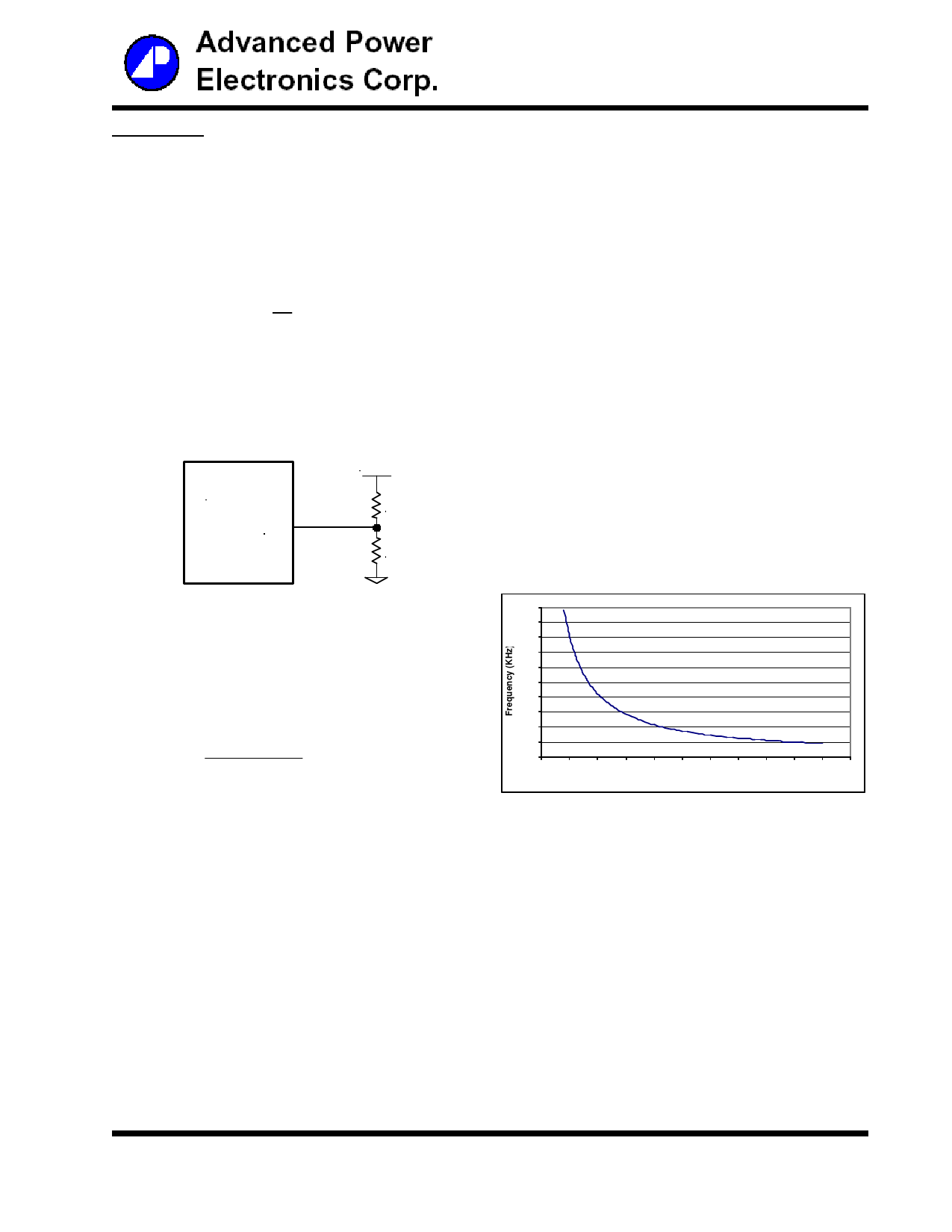
Figure 14 - Switching Frequency vs. Rt.
13/17
Share Link: 