AT17C010A-10PC View Datasheet(PDF) - Atmel Corporation
Part Name
Description
Manufacturer
AT17C010A-10PC Datasheet PDF : 15 Pages
| |||
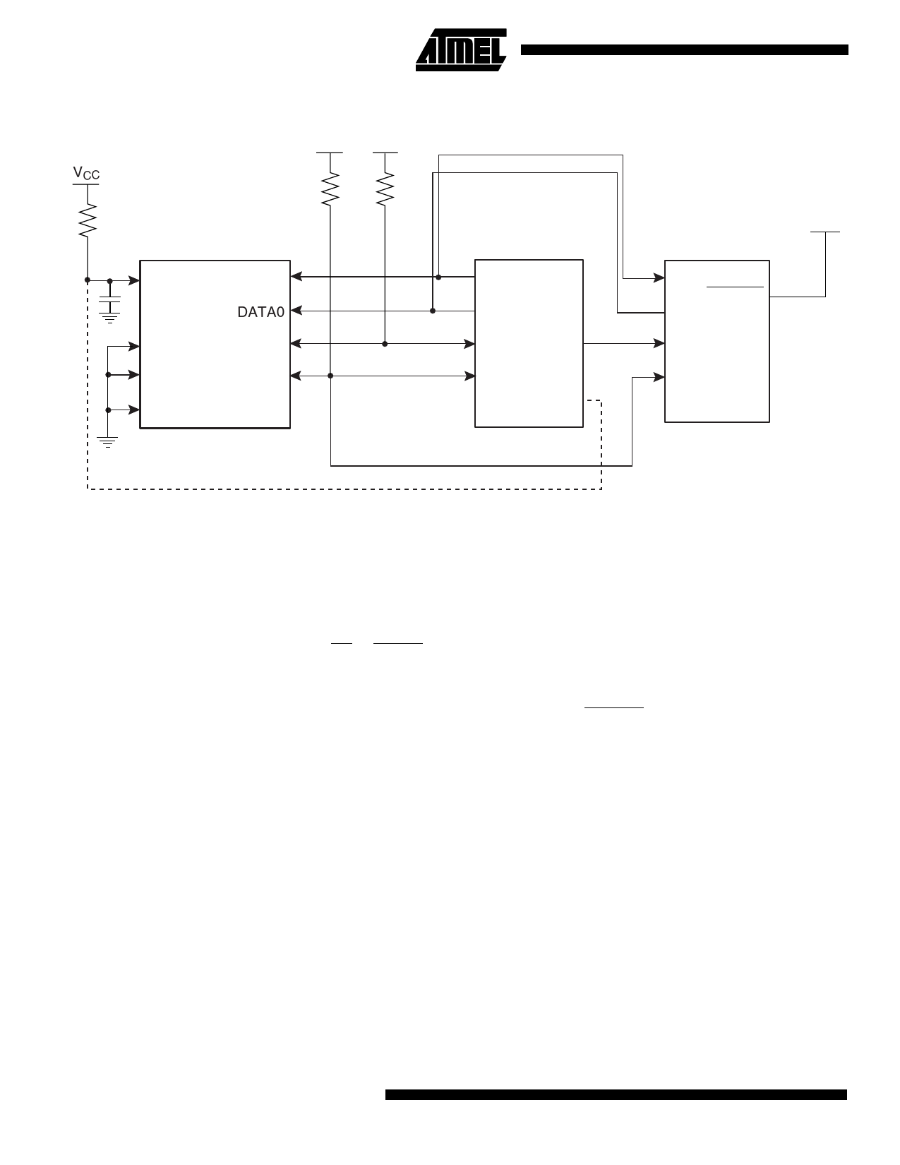
Figure 2. Configuration with Multiple AT17A Series Configurators(1)(2)(3)
VCC VCC
VCC
1 kW
EPF10K
1 kW 1 kW
AT17C512A/010A/020A
AT17LV512A/010A/020A
AT17C512A/010A/020A
AT17LV512A/010A/020A
VCC
DEVICE 1
DEVICE 2
0.1 mF
nCONFIG
DCLK
DATA0
DCLK
DATA
DCLK
SER_EN
DATA
nCE CONF_DONE
nCS nCASC
nCS
MSEL0 nSTATUS
MSEL1
OE
OE
READY
GND
Notes:
1. The use of the READY pin is optional for the 20-lead PLCC and the 32-lead TQFP packages. The 8-lead PDIP package
does not have a READY pin.
2. Introducing an RC delay to the input of nCONFIG is recommended to ensure that VCC (5V/3.3V) is reached before
configuration begins. (nCONFIG can instead be connected to an active Low system reset signal.)
3. Reset polarity of EEPROM must be set active Low (OE active High).
AT17A Series Reset
Polarity
The AT17A Series Configurator allows the user to program the reset polarity as either
RESET/OE or RESET/OE. For more details, please reference the “Programming Speci-
fication for Atmel’s FPGA Configuration EEPROMs” application note.
Programming Mode
The programming mode is entered by bringing SER_EN Low. In this mode the chip can
be programmed by the 2-wire serial interface. The programming is done at VCC supply
only. Programming super voltages are generated inside the chip. See the “Programming
Specification for Atmel’s Configuration EEPROMs” application note for further informa-
tion. The AT17A Series parts are read/write at 5V nominal. The AT17LVA Series parts
are read/write at 3.3V nominal.
Standby Mode
The AT17A Series Configurator enters a low-power standby mode whenever nCS is
asserted High. In this mode, the configuration consumes less than 0.5 mA of current at
5V. The output remains in a high-impedance state regardless of the state of the OE
input.
6 AT17C/LV512A/010A
0974E–08/01
Share Link: 