ATF-331M4 View Datasheet(PDF) - HP => Agilent Technologies
Part Name
Description
Manufacturer
ATF-331M4 Datasheet PDF : 17 Pages
| |||
ATF-331M4 Absolute Maximum Ratings[1]
Symbol
VDS
VGS
VGD
IDS
Pdiss
Pin max.
TCH
TSTG
θjc
Parameter
Drain-Source Voltage[2]
Gate-Source Voltage[2]
Gate Drain Voltage [2]
Drain Current [2]
Total Power Dissipation [4]
RF Input Power
Channel Temperature[5]
Storage Temperature
Thermal Resistance [6]
Units
V
V
V
mA
mW
dBm
°C
°C
°C/W
Absolute
Maximum
5.5
-5
-5
Idiss[3]
400
20
160
-65 to 160
200
Notes:
1. Operation of this device above any one of
these parameters may cause permanent
damage.
2. Assumes DC quiescent conditions.
3. VGS = 0 V
4. Source lead temperature is 25°C. Derate
5 mW/°C for TL > 40°C.
5. Please refer to failure rates in reliability data
sheet to assess the reliability impact of
running devices above a channel temperature
of 140°C.
6. Thermal resistance measured using 150°C
Liquid Crystal Measurement method.
500
+0.6 V
400
300
0V
200
100
-0.6 V
0
0
2
4
6
8
VDS (V)
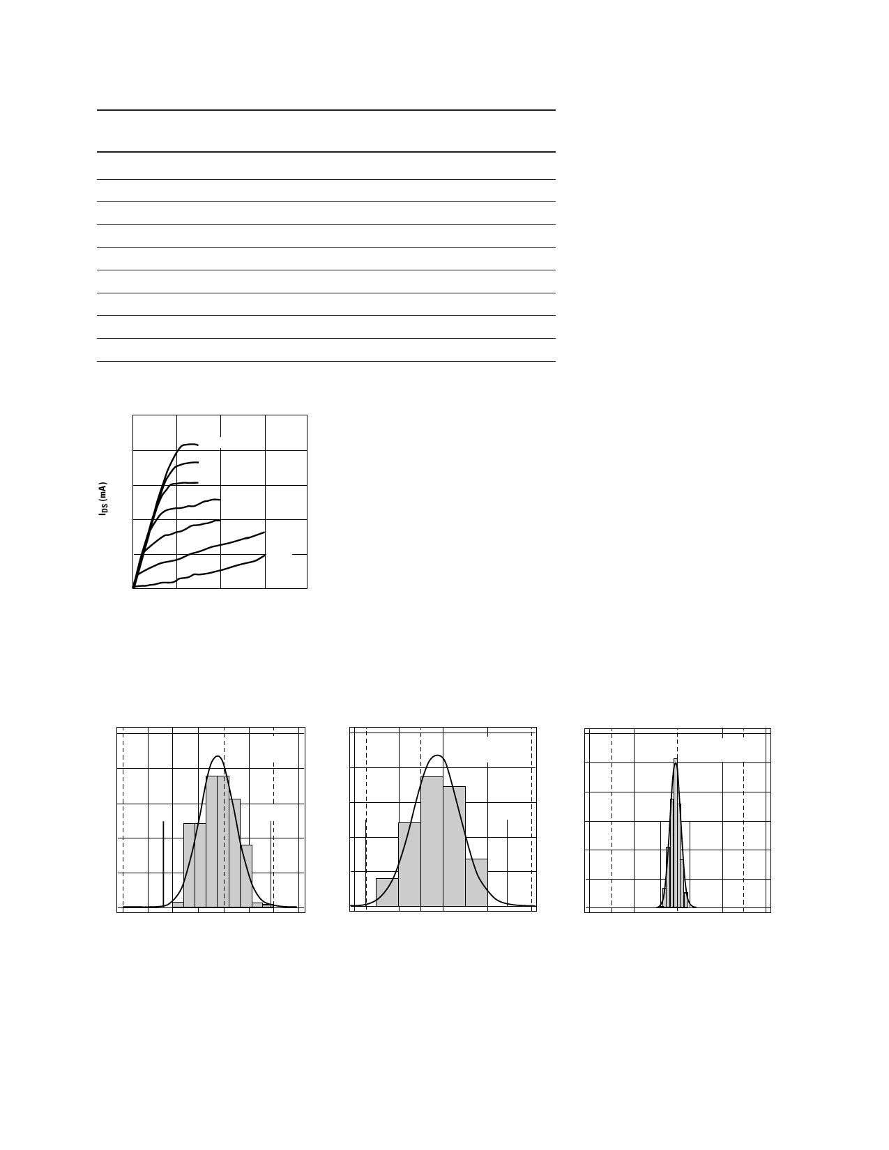
Figure 1. Typical Pulsed I-V Curves[7].
(VGS = -0.2 V per step)
Note:
7. Under large signal conditions, VGS may swing
positive and the drain current may exceed
Idss. These conditions are acceptable as long
as the Maximum Pdiss and Pin max ratings are
not exceeded.
Product Consistency Distribution Charts [8, 9]
100
80
60
-3 Std
40
20
Cpk = 1.05
Stdev = 0.07
+3 Std
150
120
90
-3 Std
60
30
120
Cpk = 1.00
Stdev = 1.07
100
80
+3 Std
60
40
20
Cpk = 4.37
Stdev = 1.11
-3 Std +3 Std
0
0.2 0.3 0.4 0.5 0.6 0.7 0.8 0.9
NF (dBm)
Figure 2. NF @ 2 GHz, 4 V, 60 mA.
LSL = 28.5, Nominal = 0.6, USL = 0.8.
0
28
30
32
34
36
OIP3 (dBm)
Figure 3. OIP3 @ 2 GHz, 4 V, 60 mA.
LSL = 28.5, Nominal = 31.0, USL = 36.0
0
13
14
15
16
17
GAIN (dB)
Figure 4. Gain @ 2 GHz, 4 V, 60 mA.
LSL = 13.5, Nominal = 15.0, USL = 16.5
Notes:
8. Distribution data sample size is 349 samples from 4 different wafers. Future wafers allocated to this product may have nominal values anywhere within
the upper and lower spec limits.
9. Measurements made on production test board. This circuit represents a trade-off between an optimal noise match and a realizeable match based on
production test requirements. Circuit losses have been de-embedded from actual measurements.
2
Share Link: 