BD9011KV-E2 View Datasheet(PDF) - ROHM Semiconductor
Part Name
Description
Manufacturer
BD9011KV-E2
ROHM Semiconductor
BD9011KV-E2 Datasheet PDF : 29 Pages
| |||
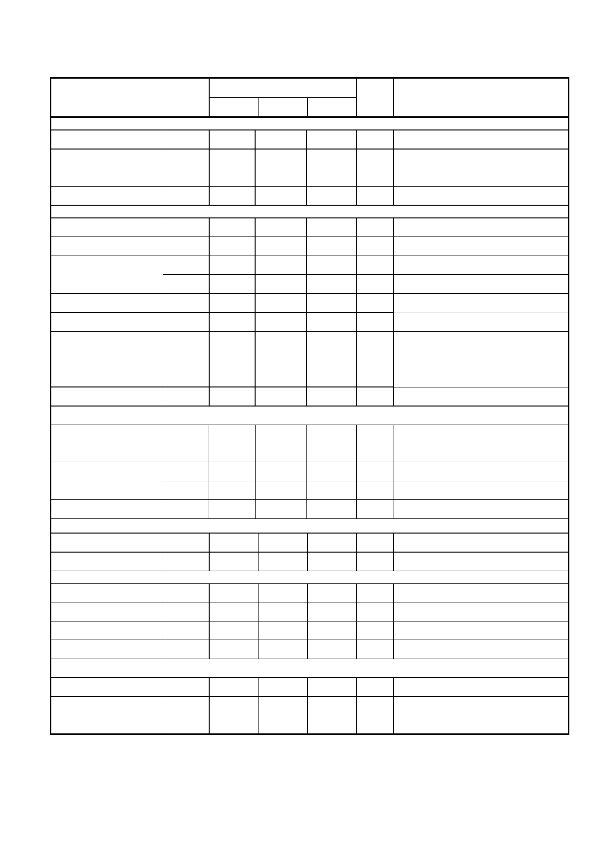
Parameter
Symbol
【PWM Comparator】
Threshold Voltage at 0%
Vth0
Threshold Voltage
at 100%
Vth100
DTC Input Bias Current
【FET Driver】
Sink Current
Idtc
Isink
Source Current
Isource
ON Resistance
RonN
RonP
Rise Time
Tr
Fall Time
Tf
Driver’s Duty Cycle of
Synchronous
ΔDuty
Rectification
SYNC Terminal Voltage Vsync
【Over Current Protection (OCP)】
Min.
0.88
1.88
-1
20
-510
7.0
0.7
-
-
42
1.45
Limits
Typ.
0.98
1.98
-
36
-320
11.0
1.4
20
100
45
1.55
VS Threshold Voltage
Vths VCC-0.24 VCC-0.21
VS Input Current
IVSH
-1
-
IVSL
-1
-
CL Input Current
【Stand-by】
Threshold Voltage
Icl
9
10
Vctl
1.0
1.5
CL Input Current
Ictl
6
15
【Short Circuit Protection (SCP)】
Timer Start Voltage
Vtime
0.6
0.7
Threshold Voltage
Vthscp
1.92
2.00
Stand-by Voltage
Vstscp
-
10
Source current
Isoscp
-4.0
-2.5
【Under Voltage Lock Out (UVLO)】
Threshold Voltage
Vuvlo
5.6
5.7
Hysteresis
Voltage Range
DVuvlo
0.05
0.1
Max.
1.08
2.08
1
58
-180
17.8
2.2
-
-
48
1.65
VCC-0.18
1
1
11
2.0
30
0.8
2.08
100
-1.5
5.8
0.15
Unit
Condition
V FB Voltage
V FB Voltage
μA
mA
mA
Ω
Ω
nsec
nsec
VDS=0.4V
VDS=0.4V
OUT1,2H,2L : L
OUT1,2H,2L : H
Switching with COUT=5000pF
Switching with COUT=5000pF
RSYNC=30KΩ,
%
50% of main driver’s duty cycle
V Rsync=30KΩ,FB=1.5V
RCL=21kΩ, the output tern off after
V
detected 8 cycle
μA VS1,VS2=PBU
μA VS1,VS2=0V
μA
V
μA CTL1,CTL2=3V
V INV Voltage
V SCP Voltage
mV SCP Voltage
μA SCP=1.0V
V Vcc sweep down
V
19/28
Share Link: 