CXA3252N View Datasheet(PDF) - Sony Semiconductor
Part Name
Description
Manufacturer
CXA3252N Datasheet PDF : 32 Pages
| |||
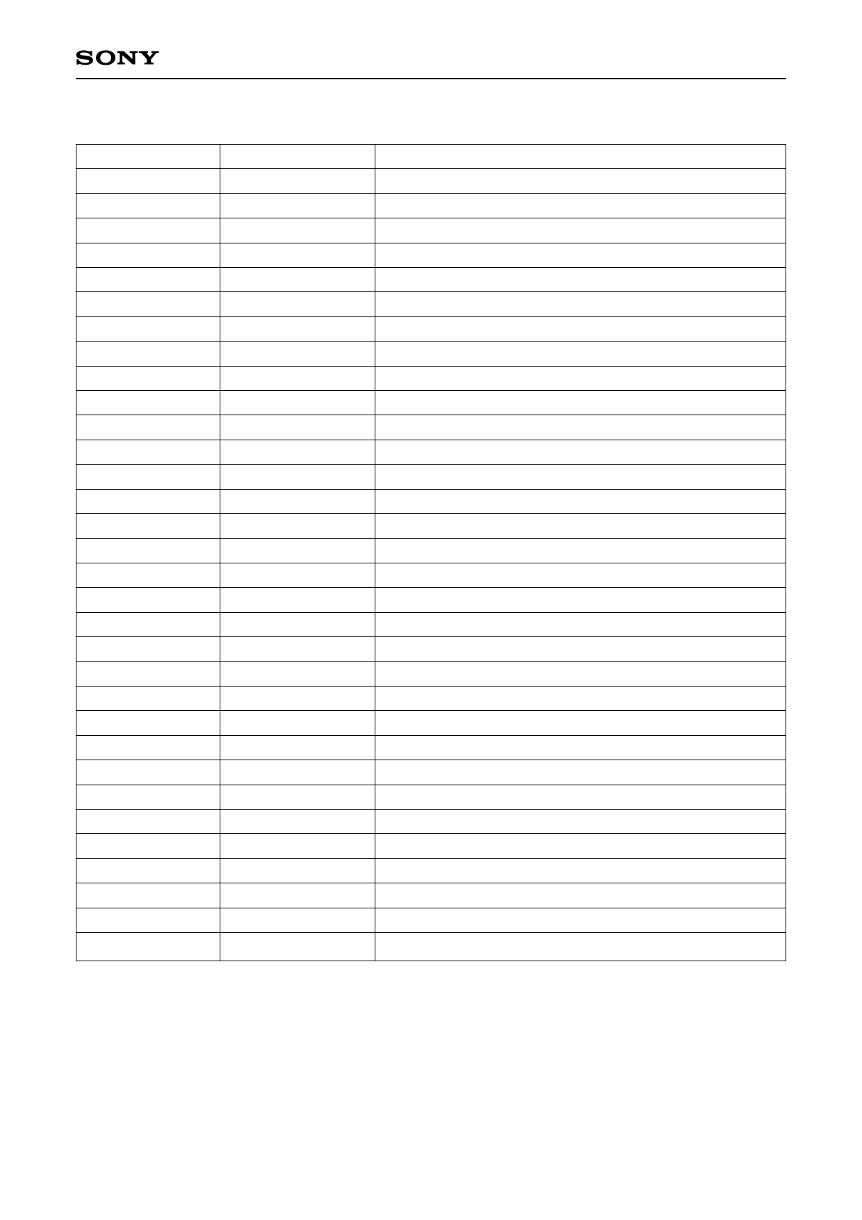
Pin Description
Pin No.
1
2
3
4
5
6
7
8
9
10
11
12
13
14
15
16
17
18
19
20
21
22
23
24
25
26
27
28
29
30
31
32
CXA3252N
Symbol
CL
DA
BS3
BS1
IFIN1
IFIN2
BS2
BS4
VCC1
MIXOUT1
MIXOUT2
GND1
BYP/MS
VHFIN
UHFIN1
UHFIN2
VOSC1
GND
VOSC2
UOSCB1
UOSCE1
UOSCE2
UOSCB2
VCC2
GND2
IFOUT
NC
VT
CPO
REFOSC
VCC3
ADSW/CE
Description
CLOCK/SCL (I2C bus)
DATA/SDA (I2C bus)
Band switch output 3
Band switch output 1 (VHF low band)
IF amplifier input 1
IF amplifier input 2
Band switch output 2 (VHF high band)
Band switch output 4
Analog circuit Vcc
MIX output (open collector)
MIX output (open collector)
Analog circuit GND
VHF input GND and control bus switching
VHF input
UHF input
UHF input
VHF oscillator (base input)
GND
VHF oscillator (collector output)
UHF oscillator (base pin)
UHF oscillator (emitter pin)
UHF oscillator (emitter pin)
UHF oscillator (base pin)
PLL circuit Vcc
PLL circuit GND
IF amplifier output
OPEN
Tuning voltage output (open collector)
Charge pump output (loop filter connection)
Crystal connection
Band switch power supply
Enable/address selection (I2C bus)
–3–
Share Link: 