CY7C057 View Datasheet(PDF) - Cypress Semiconductor
Part Name
Description
Manufacturer
CY7C057 Datasheet PDF : 23 Pages
| |||
CY7C056V
CY7C057V
Switching Characteristics Over the Operating Range[13] (continued)
Parameter
Busy Timing[19]
Description
tBHC
BUSY HIGH from CE HIGH
tPS
Port Set-Up for Priority
tWB
R/W LOW after BUSY (Slave)
tWH
R/W HIGH after BUSY HIGH (Slave)
tBDD[20]
BUSY HIGH to Data Valid
Interrupt Timing[19]
tINS
INT Set Time
tINR
INT Reset Time
Semaphore Timing
tSOP
tSWRD
tSPS
tSAA
SEM Flag Update Pulse (OE or SEM)
SEM Flag Write to Read Time
SEM Flag Contention Window
SEM Address Access Time
-12
Min. Max.
CY7C056V
CY7C057V
-15
Min. Max.
-20
Min. Max.
12
15
20
5
5
5
0
0
0
11
13
15
12
15
20
12
15
20
12
15
20
10
10
10
5
5
5
5
5
5
12
15
20
Unit
ns
ns
ns
ns
ns
ns
ns
ns
ns
ns
ns
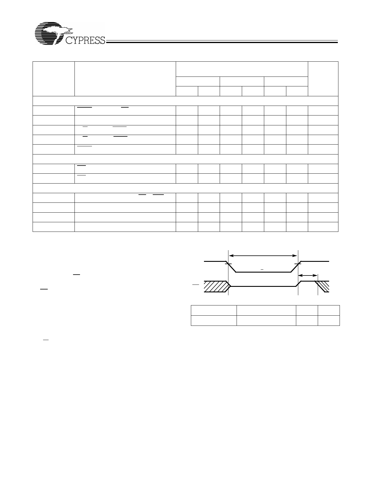
Data Retention Mode
The CY7C056V and CY7C057V are designed with battery
backup in mind. Data retention voltage and supply current are
guaranteed over temperature. The following rules ensure data
retention:
1. Chip Enable (CE)[3] must be held HIGH during data retention,
within VDD to VDD – 0.2V.
2. CE must be kept between VDD – 0.2V and 70% of VDD
during the power-up and power-down transitions.
3. The RAM can begin operation >tRC after VDD reaches the
minimum operating voltage (3.15 volts).
Timing
VCC
CE
Data Retention Mode
3.15V
3.15V
VCC > 2.0V
tRC
VCC to VCC – 0.2V
VIH
Parameter
ICCDR1
Test Conditions[21]
@ VDDDR = 2V
Max.
50
Unit
µA
Notes:
20. tBDD is a calculated parameter and is the greater of tWDD–tPWE (actual) or tDDD–tSD (actual).
21. CE = VDD, Vin = VSS to VDD, TA = 25°C. This parameter is guaranteed but not tested.
Document #: 38-06055 Rev. **
Page 10 of 23
Share Link: 