DS2441 View Datasheet(PDF) - Dallas Semiconductor -> Maxim Integrated
Part Name
Description
Manufacturer
DS2441 Datasheet PDF : 29 Pages
| |||
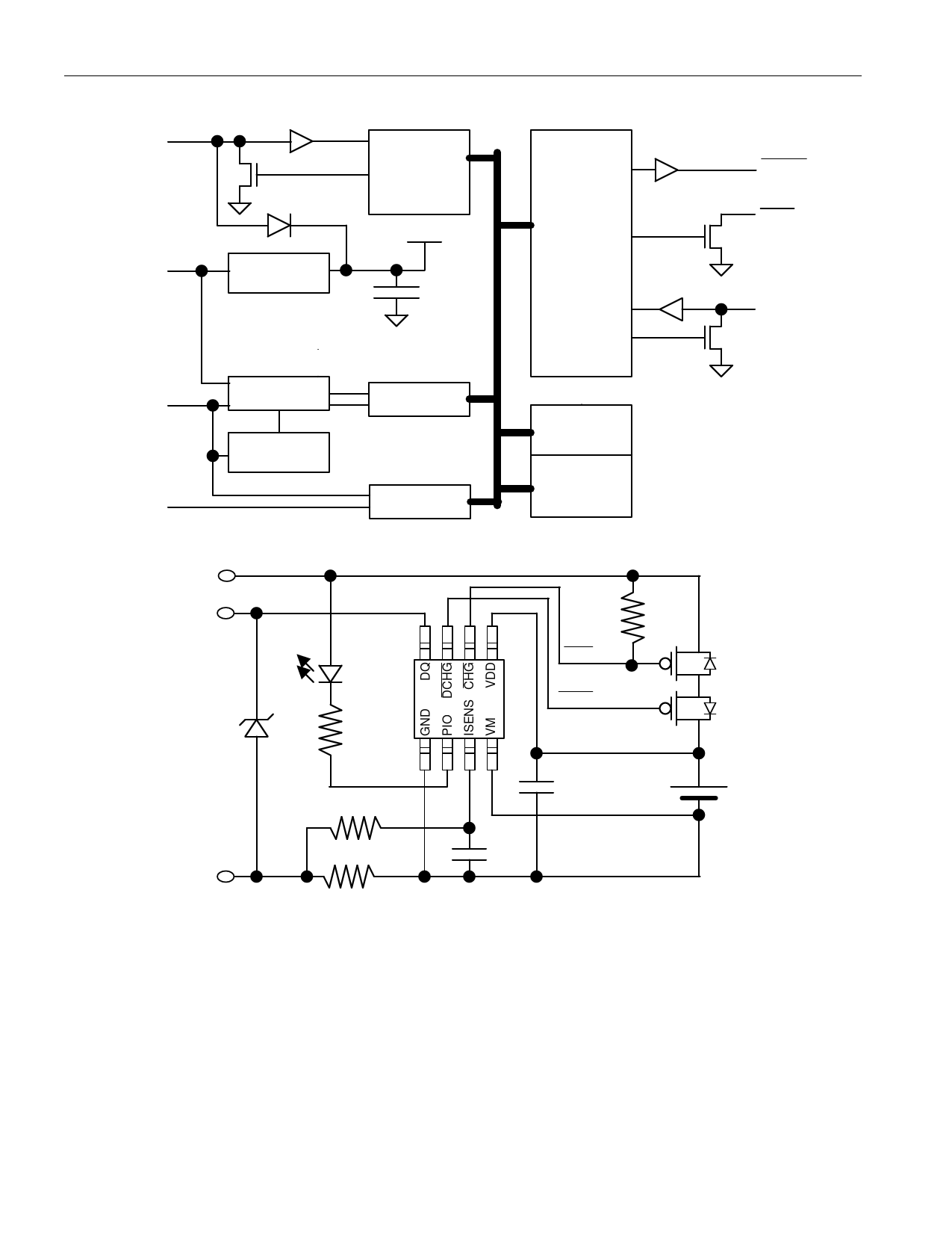
BLOCK DIAGRAM Figure 1
DQ
1-Wire I/O
and
64-bit
ROM ID
VDD
VREG
Control
Logic
DS2441
DCHG
CHG
PIO
GND
MUX
Voltage A/D
Temp
Sensor
ISENS
Current A/D
APPLICATION EXAMPLE Figure 2
PACK+
DATA
8765
DS2441
Registers
32-Byte
User
Memory
1MΩ
CHG
DCHG
6.2V
1KΩ
VDD
1234
PIO
0.1µF
Cell
2.2KΩ
VM
PACK−
0.025Ω
RSENS
0.1µF
GND
The circuit in Figure 2 depicts the DS2441 in a one-cell battery pack application. The circuit employs two
p-channel power MOSFETs as charge and discharge protection switches along with a 1 MΩ pullup
resistor to PACK+ to turn off the charge FET. The DS2441 tracks current in and out of the pack by
measuring the voltage across sense resistor RSENS (i.e., the voltage on ISENS with respect to GND). The
0.1 µF capacitor and 2.2 kΩ resistor on the ISENS pin form a low-pass filter to aid current measurement
and accumulation. The diagram shows how the PIO pin can be used to drive an LED to implement a
state-of-charge display. A zener diode limits the maximum voltage at the DQ terminal in the event that
the pullup voltage is higher than the specified maximum DQ input voltage. Although the DS2441 has a
10kV ESD rating, this diode is recommended to clamp ESD events safely outside the IC.
3 of 29
Share Link: 