EL5172(2010) View Datasheet(PDF) - Intersil
Part Name
Description
Manufacturer
EL5172 Datasheet PDF : 15 Pages
| |||
EL5172, EL5372
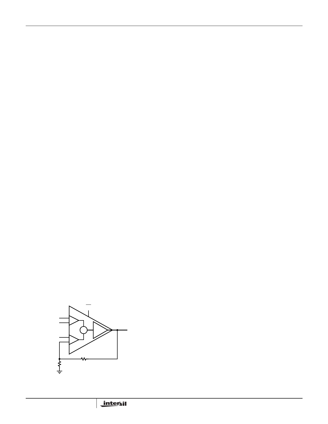
power consumption. The amplifier's power-down can be
controlled by standard CMOS signal levels at the ENABLE
pin. The applied logic signal is relative to VS+ pin. Letting the
EN pin float or applying a signal that is less than 1.5V below
VS+ will enable the amplifier. The amplifier will be disabled
when the signal at EN pin is above VS+ - 0.5V. If a TTL
signal is used to control the enabled/disabled function,
Figure 24 could be used to convert the TTL signal to CMOS
signal.
5V
10k
1k
EN
CMOS/TTL
FIGURE 24.
Output Drive Capability
The EL5172 and EL5372 have internal short circuit
protection. Its typical short circuit current is ±95mA. If the
output is shorted indefinitely, the power dissipation could
easily increase such that the part will be destroyed.
Maximum reliability is maintained if the output current never
exceeds ±60mA. This limit is set by the design of the internal
metal interconnections.
Power Dissipation
With the high output drive capability of the EL5172 and
EL5372, it is possible to exceed the +135°C absolute
maximum junction temperature under certain load current
conditions. Therefore, it is important to calculate the
maximum junction temperature for the application to
determine if the load conditions or package types need to be
modified for the amplifier to remain in the safe operating
area.
The maximum power dissipation allowed in a package is
determined according to Equation 3:
PDMAX
=
T----J---M-----A----X-----–-----T----A---M-----A----X--
ΘJA
(EQ. 3)
• TJMAX = Maximum junction temperature
• TAMAX = Maximum ambient temperature
• θJA = Thermal resistance of the package
Assuming the REF pin is tied to GND for VS = ±5V
application, the maximum power dissipation actually
produced by an IC is the total quiescent supply current times
the total power supply voltage, plus the power in the IC due
to the load, or:
For sourcing, use Equation 4:
PDMAX =
VS
×
ISMAX
+
(VS+
–
VOUT
)
×
--V-----O----U----T----
RLOAD
×i
(EQ. 4)
For sinking, use Equation 5:
PDMAX = [VS × ISMAX + (VOUT – VS- ) × ILOAD ] × i
(EQ. 5)
Where:
• VS = Total supply voltage
• ISMAX = Maximum quiescent supply current per channel
• VOUT = Maximum output voltage of the application
• RLOAD = Load resistance
• ILOAD = Load current
• i = Number of channels
By setting the two PDMAX equations equal to each other, we
can solve the output current and RLOAD to avoid the device
overheat.
Power Supply Bypassing and Printed Circuit
Board Layout
As with any high frequency device, a good printed circuit
board layout is necessary for optimum performance. Lead
lengths should be as short as possible. The power supply
pin must be well bypassed to reduce the risk of oscillation.
For normal single supply operation, where the VS- pin is
connected to the ground plane, a single 4.7µF tantalum
capacitor in parallel with a 0.1µF ceramic capacitor from VS+
to GND will suffice. This same capacitor combination should
be placed at each supply pin to ground if split supplies are to
be used. In this case, the VS- pin becomes the negative
supply rail.
For good AC performance, parasitic capacitance should be
kept to a minimum. Use of wire wound resistors should be
avoided because of their additional series inductance. Use
of sockets should also be avoided if possible. Sockets add
parasitic inductance and capacitance that can result in
compromised performance. Minimizing parasitic capacitance
at the amplifier's inverting input pin is very important. The
feedback resistor should be placed very close to the
inverting input pin. Strip line design techniques are
recommended for the signal traces.
11
FN7311.9
September 14, 2010
Share Link: 