HEF40244BDB View Datasheet(PDF) - Philips Electronics
Part Name
Description
Manufacturer
HEF40244BDB Datasheet PDF : 6 Pages
| |||
Philips Semiconductors
Octal buffers with 3-state outputs
Product specification
HEF40244B
buffers
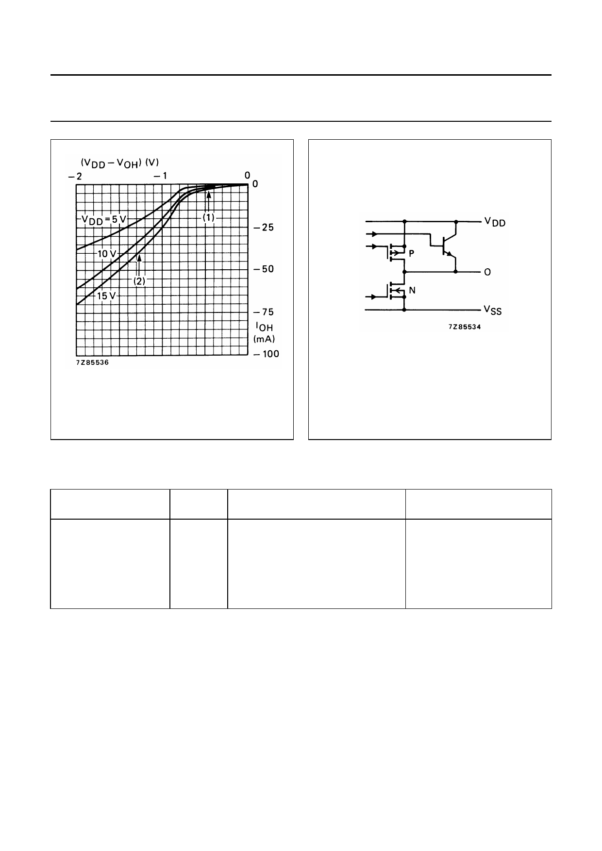
(1) P-channel MOS transistor conducting.
(2) P-channel MOS transistor and bipolar
n-p-n transistor conducting.
Fig.4 Typical output source current characteristic.
Fig.5 Schematic diagram of output stage.
AC CHARACTERISTICS
VSS = 0 V; Tamb = 25 °C; input transition times ≤ 20 ns
ALL BUFFERS
SWITCHING
Dynamic power
dissipation per
package (P)
VDD
V
TYPICAL FORMULA FOR P (µW)
5
4 250 fi + ∑ (foCL) × VDD2
10
17 000 fi + ∑ (foCL) × VDD2
15
46 000 fi + ∑ (foCL) × VDD2
where
fi = input freq. (MHz)
fo = output freq. (MHz)
CL = load capacitance (pF)
∑ (foCL) = sum of outputs
VDD = supply voltage (V)
January 1995
4
Share Link: 