HIP6004DCB-T(2000) View Datasheet(PDF) - Intersil
Part Name
Description
Manufacturer
HIP6004DCB-T
(Rev.:2000)
(Rev.:2000)
Intersil
HIP6004DCB-T Datasheet PDF : 11 Pages
| |||
HIP6004D
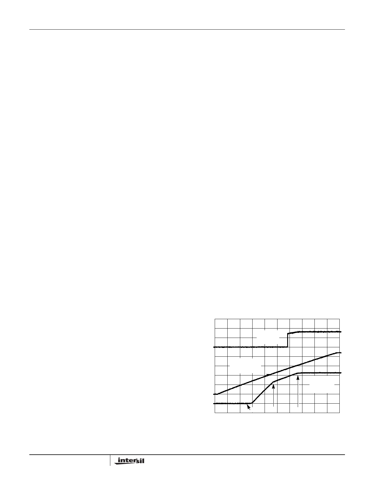
referenced to VIN) exceeds the voltage across ROCSET, the
over-current function initiates a soft-start sequence. The soft-
start function discharges CSS with a 10µA current sink and
inhibits PWM operation. The soft-start function recharges
CSS, and PWM operation resumes with the error amplifier
clamped to the SS voltage. Should an overload occur while
recharging CSS, the soft start function inhibits PWM operation
while fully charging CSS to 4V to complete its cycle. Figure 4
shows this operation with an overload condition. Note that the
inductor current increases to over 15A during the CSS
charging interval and causes an over-current trip. The
converter dissipates very little power with this method. The
measured input power for the conditions of Figure 4 is 2.5W.
The over-current function will trip at a peak inductor current
(IPEAK) determined by:
IPEAK = I--O-----C----S----E-r--D-T---S--x--(--O-R----N-O---)-C-----S----E---T--
where IOCSET is the internal OCSET current source (200µA
typical). The OC trip point varies mainly due to the
MOSFET’s rDS(ON) variations. To avoid over-current tripping
in the normal operating load range, find the ROCSET resistor
from the equation above with:
1. The maximum rDS(ON) at the highest junction temperature.
2. The minimum IOCSET from the specification table.
3. Determine IPEAK for IPEAK > IOUT(MAX) + (∆I) ⁄ 2 ,
where ∆I is the output inductor ripple current.
For an equation for the ripple current see the section under
component guidelines titled ‘Output Inductor Selection’.
A small ceramic capacitor should be placed in parallel with
ROCSET to smooth the voltage across ROCSET in the
presence of switching noise on the input voltage.
Output Voltage Program
The output voltage of a HIP6004D converter is programmed
to discrete levels between 1.100VDC and 1.850VDC. The
voltage identification (VID) pins program an internal voltage
reference (DACOUT) with a TTL-compatible 5-bit digital-to-
analog converter (DAC). The level of DACOUT also sets the
PGOOD and OVP thresholds. Table 1 specifies the DACOUT
voltage for the 32 different combinations of connections on the
VID pins. The output voltage should not be adjusted while the
converter is delivering power. Remove input power before
changing the output voltage. Adjusting the output voltage
during operation could toggle the PGOOD signal and exercise
the overvoltage protection.
‘11111’ VID pin combination resulting in a 0V output setting
activates the Power-On Reset function and disables the gate
drives circuitry. For this specific VID combination, though,
PGOOD asserts a high level. This unusual behavior has been
implemented in order to allow for operation in dual-
microprocessor systems where AND-ing of the PGOOD
signals from two individual power converters is implemented.
Application Guidelines
Layout Considerations
As in any high frequency switching converter, layout is very
important. Switching current from one power device to another
can generate voltage transients across the impedances of the
interconnecting bond wires and circuit traces. These
interconnecting impedances should be minimized by using
wide, short printed circuit traces. The critical components
should be located as close together as possible, using ground
plane construction or single point grounding.
TABLE 1. OUTPUT VOLTAGE PROGRAM
VID4
1
PIN NAME
VID3 VID2 VID1
1
1
1
VID0
1
NOMINAL OUTPUT
VOLTAGE DACOUT
0
VID4
0
PIN NAME
VID3 VID2 VID1
1
1
1
1
1
1
1
0
1.100
0
1
1
1
1
1
1
0
1
1.125
0
1
1
0
1
1
1
0
0
1.150
0
1
1
0
1
1
0
1
1
1.175
0
1
0
1
1
1
0
1
0
1.200
0
1
0
1
1
1
0
0
1
1.225
0
1
0
0
1
1
0
0
0
1
0
1
1
1
1
0
1
1
0
1.250
1.275
1.300
0
1
0
0
0
0
1
1
0
0
1
1
1
0
1
0
1
1.325
0
0
1
0
1
0
1
0
0
1.350
0
0
1
0
1
0
0
1
1
1.375
0
0
0
1
1
0
0
1
0
1.400
0
0
0
1
1
0
0
0
1
1.425
0
0
0
0
1
0
0
0
0
1.450
0
0
0
0
NOTE: 0 = connected to GND or VSS, 1 = connected to VDD through pull-up resistors.
VID0
1
0
1
0
1
0
1
0
1
0
1
0
1
0
1
0
NOMINAL OUTPUT
VOLTAGE DACOUT
1.475
1.500
1.525
1.550
1.575
1.600
1.625
1.650
1.675
1.700
1.725
1.750
1.775
1.800
1.825
1.850
6
Share Link: 