IDT72V3651 View Datasheet(PDF) - Integrated Device Technology
Part Name
Description
Manufacturer
IDT72V3651 Datasheet PDF : 21 Pages
| |||
3.3 VOLT CMOS SyncFIFOTM
512 x 36
1,024 x 36
2,048 x 36
IDT72V3631
IDT72V3641
IDT72V3651
FEATURES
• Storage capacity:
IDT72V3631 - 512 x 36
IDT72V3641 - 1,024 x 36
IDT72V3651 - 2,048 x 36
• Supports clock frequencies up to 67 MHz
• Fast access times of 10ns
• Free-running CLKA and CLKB can be asynchronous or coinci-
dent (permits simultaneous reading and writing of data on a
single clock edge)
• Clocked FIFO buffering data from Port A to Port B
• Synchronous read retransmit capability
• Mailbox register in each direction
• Programmable Almost-Full and Almost-Empty flags
• Microprocessor interface control logic
• Input Ready (IR) and Almost-Full (AF) flags synchronized by
CLKA
• Output Ready (OR) and Almost-Empty (AE) flags synchronized
by CLKB
• Available in 132-pin plastic quad flat package (PQFP) or space-
saving 120-pin thin quad flat package (TQFP)
• Pin and functionally compatible versions of the 5V operating
IDT723631/723641/723651
• Easily expandable in width and depth
• Industrial temperature range (–40°C to +85°C) is available
DESCRIPTION
The IDT72V3631/72V3641/72V3651 are pin and functionally compatible
versons of the IDT723631/723641/723651, designed to run off a 3.3V supply
for exceptionally low-power consumption. These devices are monolithic high-
speed, low-power, CMOS clocked FIFO memory. It supports clock frequencies
up to 67 MHz and has read access times as fast as 10ns. The 512/1,024/2,048
x 36 dual-port SRAM FIFO buffers data from port A to Port B. The FIFO memory
has retransmit capability, which allows previously read data to be accessed
again. The FIFO operates in First Word Fall Through mode and has flags to
indicate empty and full conditions and conditions and two programmable flags
(Almost-Full and Almost-Empty) to indicate when a selected number of words
is stored in memory. Communication between each port may take place with
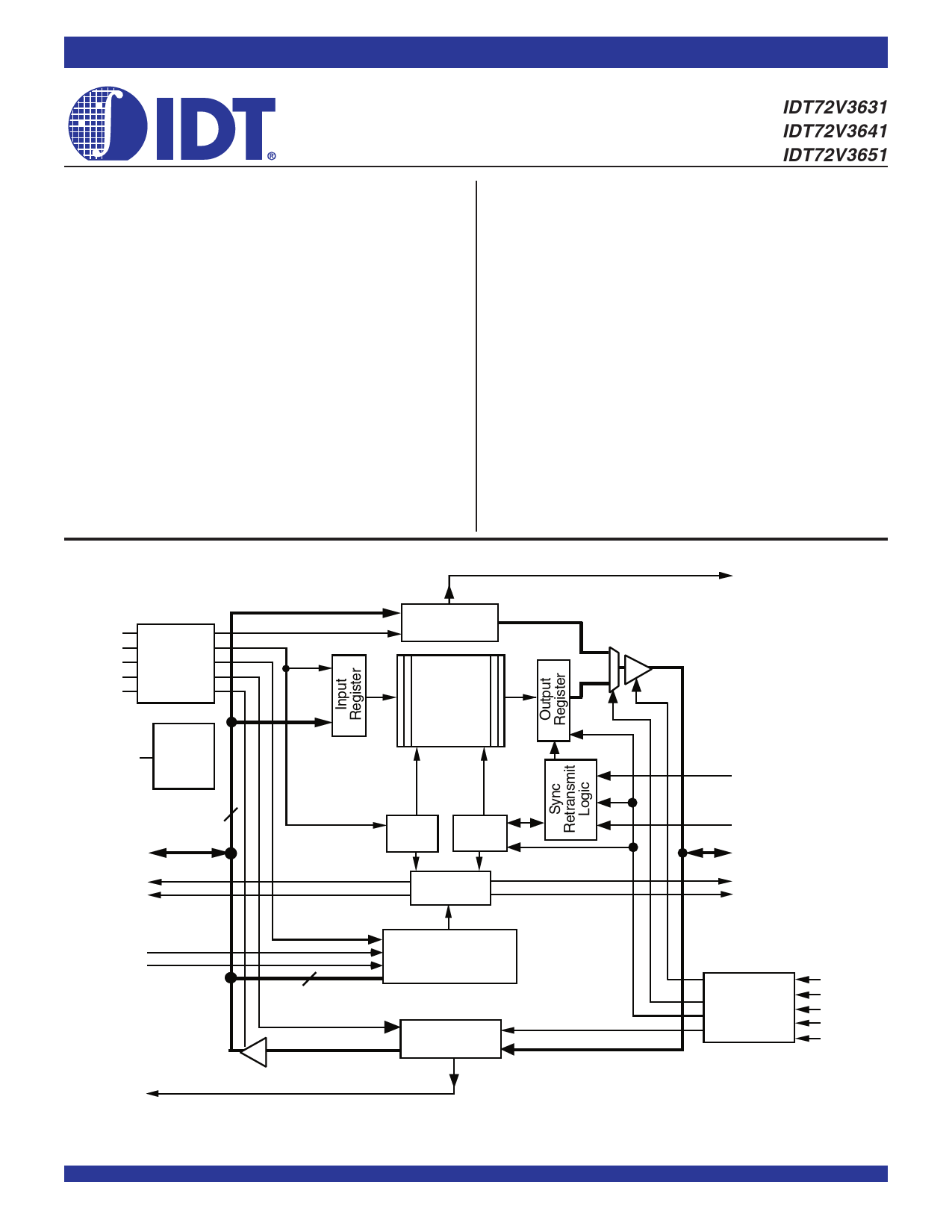
FUNCTIONAL BLOCK DIAGRAM
MBF1
CLKA
CSA
W/RA
ENA
MBA
Port-A
Control
Logic
RST
Reset
Logic
Mail 1
Register
RAM ARRAY
512 x 36
1,024 x 36
2,048 x 36
RTM
36
A0 - A35
IR
AF
Write Read
Pointer Pointer
Status Flag
Logic
RFM
B0 - B35
OR
AE
FS0/SD
FS1/SEN
Flag Offset
Registers
10
Mail 2
Register
MBF2
IDT and the IDT logo are registered trademark of Integrated Device Technology, Inc. SyncFIFO is a trademark of Integrated Device Technology, Inc.
COMMERCIAL TEMPERATURE RANGE
11
2003 Integrated Device Technology, Inc. All rights reserved. Product specifications subject to change without notice.
Port-B
Control
Logic
CLKB
CSB
W/RB
ENB
MBB
4658 drw 01
NOVEMBER 2003
DSC-4658/1
Share Link: 