IT8705F View Datasheet(PDF) - Unspecified
Part Name
Description
Manufacturer
IT8705F Datasheet PDF : 185 Pages
| |||
Revision History
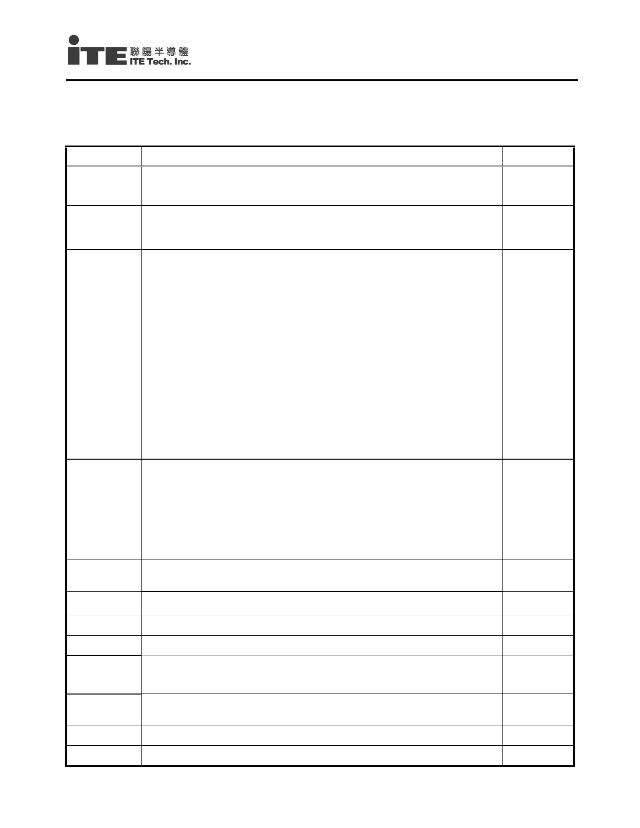
Revision History
Note: Words in bold typeface in the revisions below indicate the changes.
Section
1
2
4
5
6
8
Revision
• The feature of Flash ROM Interface was revised.
• Added a new feature “Only for IT8705AF”.
• In the fourth paragraph, “There is also a flash ROM interface with Address
(FA[0:18])” was changed into “There is also a flash ROM interface with
Address (FA[0:19])”.
• Pin 26 was revised to “FA10/VID_O5/GP32”.
• Pin 27 was revised to “FA11/VID_I5/GP33”.
• Pin 49 was revised to “JSACX/GP40/FAN_TAC1S 5”.
• Pin 50 was revised to “JSACY/GP41/ FAN_TAC2S”.
• Pin 51 was revised to “JSAB1/GP42/ FAN_TAC3S”.
• Pin 52 was revised to “JSAB2/GP43/ FAN_CTL3S”.
• Pin 55 was revised to “JSBB1/GP46/ FAN_CTL1S”.
• Pin 56 was revised to “JSBB2/GP47/ FAN_CTL2S”.
• Pin 61 was revised to “DRVB#/SCCLK/FA19”.
• Pin 87 was revised to “TMPIN3/COPEN#”.
• Pin 91 was revised to “VIN7/TMPIN3”.
• In table 5-3, the signal and description of pin 91 and 87 were revised.
• In table 5-7, the signal, attribute and description of pin 49 to 52 and pin 55
to 56 were revised.
• In table 5-10, the signal, attribute and description of pin 61 were revised.
• In table 5-11, the signal, attribute and description of pin 26 to 31 were
revised.
• In section six, the signal and description of pin 26, 27, 49 to 52, 55, 56
and 80 were revised.
• In table 8-1, index 2Bh was added.
• In table 8-7, index D8h, D9h and DAh were added.
• In section 8.3.5, the default value was changed into “03h”
• In section 8.3.6, the description of bit 5 was revised.
• In section 8.3.7, the description of bit 1 was revised.
• Section 8.3.14 GPIO Set 4 Alternate Multi-Function Pin Selection Register
(Index=2Bh, Default=00h) was added.
• In section 8.5.5, 8.6.5 and 8.6.6, the description of bit 3 was revised.
• In section 8.8.10, the description of bit 2 was revised.
Page No.
1
3
7
10-18
22-23
28
32
35
36
42
45-47
52
www.ite.com.tw
1
IT8705F V0.4
Share Link: 